
Design Techniques for EMC Part 4: ShieldingBy Eur Ing Keith Armstrong C.Eng MIEE MIEEE |
This is the fourth in a series of six articles on best-practice EMC techniques in electrical/electronic/mechanical hardware design, to be published in this journal over the current year. The series is intended for the designer of electronic products, from building block units such as power supplies, single-board computers, and "industrial components" such as motor drives, through to stand-alone or networked products such computers, audio/video/TV, instruments, etc.
The techniques to be covered in the six articles are:
The important point is that shielding can be very low cost if it is designed-in carefully from the start, but can be extremely expensive indeed if it has to be applied at the last minute to make a product acceptable to a customer (or to an EMC enforcement agent).
Shielding always adds cost and weight, so it is always best to use the other techniques described in this series to improve EMC and reduce the need for shielding. Even where it is hoped to avoid shielding altogether it is best to allow for Murphy's Law and design from the start so that shielding can be added later if necessary. Mr Murphy can usually be discouraged from upsetting your product roll-out if you have a variety of shielding (and filtering) solutions ready to be dropped in when you first test your new product for EMC.
A degree of shielding can also be achieved by keeping all conductors and components very close to a solid metal sheet. Ground-planed PCBs populated entirely by low-profile surface mounted devices are therefore recommended for their EMC advantages. Even though such PCBs may require additional enclosure (volumetric) shielding, it should not need to have as high a shielding effectiveness (SE) and so will be easier to make and cost less.
A useful degree of shielding can be achieved in electronic assemblies by keeping their internal electronic units and cables very close to an earthed metal surface at all times, and bonding their earths directly to it instead of (or as well as) using a safety star earthing system based on green/yellow wires. This technique usually uses zinc-plated mounting plates or chassis, and can help avoid the need for high values of enclosure SE.
At thicknesses of 0.5mm or over, most normal fabrication metals provide good SE above 1MHz and excellent SE above 100MHz. Problems with metal shields are mostly caused by thin materials, frequencies below 1MHz, and apertures, and this article focuses mainly on these.
Where enclosures have parallel walls opposite each other standing waves can build up at resonant frequencies, and these can cause SE problems. Irregular shaped enclosures, or ones with curved or non-parallel walls (more hollow laughter) will help prevent resonances. Where opposing shield walls are parallel, try to prevent the resonances due to the width, height, or length from occurring at the same frequencies. So avoid cubic enclosures, use rectangular cross-sections instead of square, and try to avoid dimensions that are simple multiples of each other. E.g. if the length is 1.5 times the width, the second resonance of the width coincides with the third resonance of the length. Best to use irrationally ratio'd dimensions, such as that provided by the venerable Fibonacci series (which the Greeks knew as the Golden Mean). It is probably not worth worrying too much about this because the internal PCBs, components, and wiring alter its resonances unpredictably anyway.
However, magnetic fields are much more difficult to stop. They need to generate eddy currents inside the shield material to create magnetic fields that oppose the impinging field. Thin aluminium is not going to be very suitable for this purpose, and the depth of current penetration required for a given SE depends on the frequency of the field, and on the characteristics of the metal used for the shield, and is known as the "skin effect".
One skin depth is the depth in the shield material at which the "skin effect" causes the currents caused by the impinging magnetic field to be reduced by approximately 9dB. So a material which was as thick as 3 skin depths would have an approximately 27dB lower current on its opposite side and have an SE of approximately 27dB for that M field.
Skin effect is especially important at low frequencies, where the fields experienced are more likely to be predominantly magnetic with a lower wave impedance than 377W. The formula for skin depth is given in most textbooks, but requires knowledge of the shielding material's conductivity and relative permeability. Figure 4B solves this for aluminium and steel, with copper thrown in for comparison. Pure zinc will have skin depths close to those of aluminium.
Copper and aluminium have over 5 times the conductivity of steel, so are very good at stopping electric fields, but have a relative permeability of 1 (the same as air). Typical mild steel has a relative permeability of around 300 at low frequencies, falling to 1 as frequencies increase above 100kHz, and its higher permeability gives it a reduced skin depth, making reasonable thicknesses of mild steel better than aluminium for shielding low frequencies. Different grades of steels (especially stainless) have different conductivities and permeabilities, and their skin depths will vary considerably as a result.
A good material for a shield will have high conductivity and high permeability, and sufficient thickness to achieve the required number of skin depths at the lowest frequency of concern. 1mm thick mild steel plated with pure zinc (say, 10 microns or more) is fine for many applications.
In practice, whether shielding is being done to reduce emissions or improve immunity, most shield performance is limited by the apertures in it, as these two simple figures 4C and 4D try to show.


Considering apertures as holes in an otherwise perfect shield implies that they act as half-wave resonant "slot antennae", and this allows us to make predictions about maximum aperture sizes for a given SE. In practice this assumption may not always be accurate, but it has the virtue of being an easy design tool that is better than doing nothing. Where this rule turns out to be are inaccurate, it may be possible to refine it following practical experiences with the technologies and construction methods used on specific products.
The resonant frequency of a slot antenna is governed by its longest dimension - its diagonal. It makes little difference how wide or narrow an aperture is, or even whether there is a line-of-sight through the aperture. Even apertures the thickness of a paint or oxide film, formed by overlapping metal sheets, still radiate (leak) at their resonant frequency as well as if they were wide enough to poke a finger through.
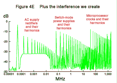
Figures 4D and 4E have been used before in this series to try to give a feel for the fact that the frequencies inside modern electronic products use the same range of frequencies as we rely on for communications and broadcasting. One of the most important EMC issues is keeping the products' internal frequencies inside, so they don't pollute the radio spectrum outside. Figure 4F shows how effective apertures in shields can be at behaving like antennas and allowing the internal frequencies to disturb the radio spectrum and cause interference.


The half-wave resonance of slot antennae is the basis for the solid line in figure 4F (and for the rule-of-thumb of figure 4G) using the relationship v = fl (where v is the speed of light: 3.108 metres/sec, f is the frequency in Hz, and l is the wavelength in metres). We find that a narrow 430mm long gap along the front edge of a 19-inch rack unit's front panel will be half-wave resonant at around 350MHz. At this frequency our example 19-inch front panel is no longer providing much shielding, and removing it entirely might not make much difference.
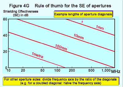
Figure 4G is useful when estimating the maximum size of an aperture for a given SE, and may be easily scaled to suit different dimensions. For an SE of 20dB at 1GHz (the present upper limit of testing in most standards) figure 4G suggests an aperture no larger than around 16 mm. For 40dB this would be only 1.6 mm, requiring gaskets to seal apertures and/or the use of the waveguide below cutoff techniques described later.
Actual SE in practice will depend on internal resonances between the walls of the enclosure itself, the proximity of components and conductors to apertures (keep noisy cables such as ribbon cables carrying digital busses well away from shield apertures and joints), the impedances of the fixings used to assemble the parts of the enclosure, etc.
Wherever possible, break all necessary or unavoidable apertures into a number of smaller ones. Unavoidably long apertures (covers, doors, etc) may need conductive gaskets or spring fingers (or other means of maintaining shield continuity). The SE of a number of small identical apertures near to each other is (crudely) proportional to the square root of their number, so two apertures will be worse by 3dB, four by 6dB, eight by 9dB, and so on. But when the wavelength at the frequency of concern starts to become comparable with the overall size of the array of small apertures, or when apertures are not near to each other (compared with the wavelength), this crude '3dB per doubling' rule breaks down because of phase cancellation effects. However, at least this simple rule errs on the side of caution.
Apertures placed more than half a wavelength apart do not in general worsen the SEs that each achieves individually, but half a wavelength at 100MHz is 1.5 metres, so at such low frequencies on typical products smaller than this an increased number of apertures will tend to worsen the enclosure's SE. Apertures don't merely behave as slot antennae. Currents flowing in a shield and forced to divert from their ideal path because there is an aperture in it will cause the aperture to emit magnetic fields. Voltage differences across an aperture will cause the aperture to emit electric fields. The author has seen dramatic levels of emissions at 130MHz from a hole no more than 4mm in diameter (intended for a click-in plastic mounting pillar) in a small PCB-mounted shield over a micro-controller. Figure 4G implies quite a good SE at that frequency from a 4mm hole, but the emissions from a particularly noisy microcontroller were causing significant currents to flow in the shielding can, and it appeared to be these that were causing the emissions, not the hole's antenna effect. Where long narrow apertures are concerned, it is sometimes possible to reduce such emissions by orienting the aperture's longer dimension appropriately with respect to the internal circuitry.
Special materials such as Mumetal and Radiometal have very high relative permeabilities, often in the region of 10,000. Their skin depth is correspondingly very small, but they are only effective up to a few tens of kHz. Care must be taken not to knock items made of these materials, as this ruins their permeability and they have to scrapped or else re-annealed in a hydrogen atmosphere. These exotic materials are used rather like channels to divert the magnetic fields away from the volume to be protected - a different concept to that used by ordinary shielding.
All metals shield materials with relative permeability greater than 1 can saturate in intense magnetic fields, and then don't work well as shields and often heat up. A steel or Mumetal shield box over a mains transformer, to reduce its hum fields, can saturate and fail to achieve the desired effect. Often, all that is necessary is to make the box larger so it does not experience such intense local fields.
Another shielding technique for low frequency shielding is active cancellation, and at least two companies have developed this technique specifically for stabilising the images of CRT VDUs in environments polluted by high levels of power frequency magnetic fields.

Figure 4H shows that if we extend the distance that a wave leaking through an aperture has to travel between surrounding metal walls before it reaches freedom, we can achieve respectable SEs despite apertures large enough to put your fist through. This very powerful technique is called "waveguide below cutoff". Honeycomb metal constructions are really a number of waveguides below cutoff stacked side-by-side, and are often used as ventilation grilles for shielded rooms, and similar high-SE enclosures.
Like any aperture, a waveguide allows all its impinging fields to pass through when its internal diagonal (g) is half a wavelength, so the cutoff frequency of our waveguide is given by:
fcutoff = 150,000/g (answer in MHz when g is in mm).
Below its cutoff frequency, a waveguide does not leak like an ordinary aperture (as shown by figure 4H) and can provide a great deal of shielding: for f<0.5fcutoff the SE achieved is approximately 27d/g, where d is the distance through the waveguide that the wave has to travel before it is free.

Figure 4J shows examples of the SE achieved by six different sizes of waveguide below cutoff. Smaller diameter (g) results in a higher cutoff frequency, with a 50mm (2 inch) diameter achieving full attenuation by 1GHz. Increased depth (d) results in increased SE, with very high values being readily achieved.
Waveguides below cutoff do not have to be made out of tubes, and can be realised using simple sheet metalwork which folds the depth (d) so as not to increase the size of the product too much. As a technique it is only limited by one's imagination, but it must be taken into consideration early in a project as it is usually difficult to retrofit.
Conductors should never be passed through waveguides below cutoff, as this compromises their effectiveness. Waveguides below cutoff can be usefully applied to plastic shafts (e.g. control knobs) so that they do not compromise SE where they exit an enclosure. The alternative is to use metal shafts with a circular conductive gasket and suffer the resulting friction and wear.
Waveguides below cutoff can avoid the need for continuous strips of gasket, and/or for multiple fixings, and thus save material costs and assembly times, but they appear to be rarely used: as a mechanical technique it is not of interest to electronic designers; and whoever saw a mechanical designer attend an EMC course?

It is worth noting in passing that the green/yellow wire used for safety earthing of a door or panel has no benefits for EMC, above a few hundred kHz. This might be extended to a few MHz if a short wide earthing strap is used instead of a long wire.
A huge range of gasket types is available from a number of manufacturers, most of whom also offer customising services. This observation reveals that no one gasket is suitable for a wide range of applications. Considerations when designing or selecting gaskets include:

Gasket contact areas must not be painted (unless it is with conductive paint), and the materials used and their preparation and plating must be carefully considered from the point of view of galvanic corrosion.
All gasket details and measures must be shown on manufacturing drawings, and all proposed changes to them assessed for their impact on shielding and EMC. It is not uncommon, when painting work is transferred to a different supplier, for gaskets to be made useless because masking information was not put on the drawings. Changes in the painting processes used can also have a deleterious effect (as can different painting operatives) due to varying degrees of overspray into gasket mounting areas which are not masked off.

Figure 4M shows a display unit mounted in a large aperture in the wall of the shielded enclosure, using an internal "dirty box" to control the field leakage through the aperture. The joint between the dirty box and the inside of the enclosure wall must be treated the same as any other joint in the shield.
Shielded windows are needed where a display needs shielding by a product's enclosure. Trinitron type CRTs are usually surprisingly well shielded (due to their substantial shadow mask) as long as the metal frame around the front of their tube is electrically bonded to the front panel all around the aperture. Active matrix LCDs upgrades to products which had used Trinitron type CRTs have been known to be the cause of more emissions than the CRTs, and some have needed additional shielded windows where the CRTs had not.
A variety of shielded windows are available, based on two main technologies:
A vital issue for screened windows is that their conducting layers (mesh, film, or honeycomb metal) must be bonded directly to the enclosure shield surface around all the edges of their cut -out. Figure 4N shows one typical assembly method, which can use a conductive sealants / glues to avoid the need for mechanical fixings. The use of UV-curable conductive adhesives can make assembly times equal to, or better than, mechanical fixing methods.

The mesh size must be small enough not to reduce the enclosure's SE too much. The SE of a number of small identical apertures near to each other is (crudely) proportional to the square root of their number, so two apertures will make SE worse by 3dB, four by 6dB, eight by 9dB, and so on. For a large number of small apertures typical of a ventilation grille, mesh size will be considerably smaller than one aperture on its own would need to be for the same SE. At higher frequencies where the size of the ventilation aperture exceeds one-quarter of the wavelength, this crude "3dB per doubling" formula can lead to over-engineering, but no simple rule of thumb exists for this situation.
Waveguides below cutoff allow high air flow rates with high values of SE, and honeycomb metal ventilation shields (consisting of many long narrow hexagonal tubes bonded side-by-side) have been used for this purpose for many years. It is believed that at least one manufacturer of highly shielded 19" rack cabinets claims to use waveguide below cutoff shielding of the top and bottom ventilation apertures using ordinary sheet metalwork techniques.
The design of shielding for ventilation apertures can be complicated by the need to clean the shield of the dirt deposited on it from the air. Careful air filter design can allow ventilation shields to be welded or otherwise permanently fixed in place.
It is often found - when it is discovered that shielding is necessary - that the design of the plastic enclosure does not permit the required SE to be achieved by coating its inner surfaces. The weak points are usually the seams between the plastic parts: they often cannot ensure a leak-tight fit, and usually cannot easily be gasketted. Expensive new mould tools are often needed, with consequent delays to market introduction and to the start of income generation from the new product.
Whenever a plastic case is required for a new product, it is financially vital that consideration be given to achieving the necessary SE right from the start of the design process.
Paint or plating on plastic can never be very thick, so the number of skin-depths achieved can be quite small. Some clever coatings using nickel and other metals have been developed to take advantage of nickel's reasonably high permeability to reduce skin depth and achieve better SE.
Other practical problems with painting and plating include making them stick to the plastic substrate over the life of the product, in its intended environment. Not easy to do without expert knowledge of the materials and processes. Conductive paint or plating flaking off inside a product can do a lot more than compromise EMC - it can short conductors out, causing unreliable operation and risking fires and electrocution. Painting and plating plastics must be done by experts with long experience in that specialised field.
A special problem with painting or plating plastics is voltage isolation. For Class II products (double insulated) adding a conductive layer inside their plastic cases can reduce creepage and clearance distances and compromise electrical safety. Also, for any plastic-cased product, adding a conductive layer to the internal surface of the case can encourage personnel electrostatic discharge (ESD) to occur through seams and joints, possibly replacing a problem of radiated interference with one of susceptibility to ESD. For commercial reasons it is important that careful design of the plastic enclosure occurs from the beginning of the design process, if there is any possibility that shielding might eventually be required.
Some companies box clever (pun intended) by using thin and unattractive low-cost metal shields on printed circuit boards or around assemblies, making it unnecessary for their pretty plastic case to do double duty as a shield. This can save a great deal of cost and headache, but must be considered from the start of a project or else there will be no room available (or the wrong type of room) to fit such internal metalwork.
Materials based on carbon fibres (which are themselves conductive) and self-conductive polymers are starting to become available, but they do not have the low conductivity of metal and so do not give as good an SE for a given thickness.
Small products with dimensions less than 0.5 metres usually make relatively inefficient antenna below 30MHz, and most problems are due to leaky cable screens (cables usually being long enough to be good antennae below 30 MHz). However, even a small product might need enclosure shielding that is effective at under 30MHz if it contains a powerful source of low-frequency fields.
The screens and connectors (or glands) of all screened cables that penetrate a shielded enclosure, and their 360§ bonding, are as vital a part of any "Faraday Cage" as the enclosure metalwork itself. The thoughtful assembly and installation of filters for unshielded external cables is also vital to achieve a good SE. These points were made in Parts 2 and 3 of this series, and they are worth making again.
In passing it is worth repeating that a cable screen pigtailed to an enclosure shield (instead of being 360§ bonded) will ruin the SE of that enclosure from quite low frequencies upwards (say, above 10MHz for a short pigtail, lower if it is longer).
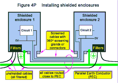
Refer to the draft IEC1000-5-6 (95/210789 DC from BSI) for best practices in industrial cabinet shielding (and filtering) and BS IEC 61000-5-2:1998 for best practices in cabling (and earthing) -including why pigtails are best consigned to the history books along with soldering irons that had to be heated in a fire. Figure 4P shows the main points of installing shielded cabinets according to these two best-practice standards, and is repeated from Part 2 of this series. Refer to Part 2 for more details on this figure as regards the installation of shielded cabling, and Part 3 for details of installing filters on unshielded cables.
The ideal PCB-level shield is a totally enclosing metal box with shielded connectors and feedthrough filters mounted in its walls, really just a miniature version of a product-level shielded enclosure as described above. The result is often called a module, can provide extremely high SEs, and is very often used in the RF and microwave worlds.
Lower cost PCB shields are possible, although their SE is not usually as good as a well-designed module. All depend upon a ground plane in a PCB being used to provide one side of the shield, so that a simple five-sided box can be assembled on the PCB like any other component. Soldering this five-sided box to the ground plane at a number of points around its circumference creates a "Faraday cage" around the desired area of circuitry. A variety of standard five-sided PCB-mounted shielding boxes are readily available, and companies who specialise in this kind of precision metalwork often make custom designs. Boxes are available with snap-on lids so that adjustments may easily be made, test points accessed, or chips replaced, with the lid off. Such removable lids are usually fitted with spring-fingers all around their circumference to achieve a good SE when they are snapped in place.
Weak points in this method of shielding are obviously the apertures created by the gaps between the ground-plane soldered connections, by any apertures in the ground plane (e.g. clearances around through-leads and via holes), and any other apertures in the five-sided box (e.g. ventilation, access to adjustable components, displays, etc.). Seam-soldering the edges of a five-sided box to a component-side ground plane can remove one set of apertures, at the cost of a time-consuming manual operation.
For the lowest cost, we want to bring all our signals and power into the shielded area of our PCB as tracks, avoiding wires and cables. This means we need to use the PCB equivalents of bulkhead-mounting shielded connectors, and bulkhead-mounting filters.
The PCB track equivalent of a shielded cable is a track run between two ground planes, often called a "stripline". Sometimes guard tracks are run on both sides of this "shielded track" on the same copper layer, these guard tracks having very frequent via holes bonding them to the top and bottom ground planes. The number of via holes per inch is the limiting factor here, as the gaps between them act as shield apertures (the guard tracks have too much inductance on their own to provide a good SE at high-frequencies). Since the dielectric constant of the PCB material is roughly four times that of air, when figures 4F and 4G are used to determine via spacing their frequency axes should be divided by two (the square root of the PCB's dielectric constant). Some designers don't bother with the guard tracks and just use via holes to "channel" the track in question. It may be a good idea to randomly vary the spacings of such rows of via holes around the desired spacing, to help avoid resonances.
Where striplines enter an area of circuitry enclosed by a shielded box, it is sufficient that their upper and lower ground planes (and any guard tracks) are bonded to the screening can's soldered joints on both sides, close to the stripline.
Tracks which only have a single ground plane layer in parallel, their other side being exposed to the air, are said to be of "microstrip" construction. When a microstrip enters a shielded PCB box it will suffer an impedance discontinuity due to the wall of the box. If the wavelength of the highest frequency component of the signals in the microstrip is greater than 100 times the thickness of the box wall (or the width of box mounting flange), the discontinuity may be too brief to register. But where this is not the case some degradation in performance may occur, and such signals are best routed using striplines.
All unshielded tracks must be filtered as they enter a shielded PCB area. It is often possible to get valuable improvements using PCB shielding without such filtering, but this is difficult to predict so filtering should always be designed-in (at least on prototypes, only being removed from the PCB layout after successful EMC testing).
The best filters are feedthrough types, but to save cost we need to avoid wired types. Leaded PCB-mounting types are available which can be soldered to a PCB in the usual manner and then hand-soldered to the wall of the screening box when it is fitted at a later stage. Quicker assembly can be achieved by soldering the central contact of the filter to the underlying ground plane, making sure that solder joints between the shielding box and the same ground plane layer are close by, on both sides. This latter construction also suits surface-mounted "feedthrough" filters, further reducing assembly costs.
But feedthrough filters, even surface mounted types, are still more expensive than simple ferrite beads or capacitors. To allow the most cost-effective filters to be found during development EMC testing, whilst also minimising delay and avoiding PCB layout iterations, multipurpose pad patterns can easily be created to take any of the following filter configurations:
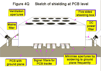
By now it should go without saying that all these PCB mounted filters should ideally be lined-up with their centres along the line of the wall of the shielding box, which will probably need a little cut-out in it to accommodate the components. Using surface-mounted devices rather than leaded allows the box cut-out size to be minimised, improving SE. Where simple lines of filters are hard to achieve, take great care not to allow any unfiltered tracks to run close to any filtered tracks. Figure 4Q attempts to sketch what low-cost PCB shielding could look like.
As with cables, it may be necessary to use shielding and filtering together, so it may be a wise precaution to provide for multi-padded filter layouts for all the "shielded" tracks entering a shielded PCB area, or at least make provision for a ferrite bead.
Keith Armstrong is a partner of Cherry Clough Consultants and an associate of EMC-UK.
He can be contacted on:
Phone: 01457 871 605
Fax: 01457 820 145
eMail: karmstrong@iee.org
Editors Note: Keith is writing a book with Tim Williams on "EMC for Systems and Installations", to be published by Butterworth-Heinemann in September 1999.
 © Nutwood UK Ltd 2001 |
Eddystone Court - De Lank Lane St Breward - BODMIN - PL30 4NQ Tel: +44 (0)1208 851530 - Fax: +44 (0)1208 850871 nutwooduk@nutwood.eu.com |
|
|
|