Design Techniques for EMC
Part 5: PCB Design and Layout
By Eur Ing Keith Armstrong C.Eng MIEE MIEEE
|
This is the fifth in a series of six articles on best-practice EMC techniques in electrical/electronic/mechanical hardware design, to be published in this journal over the current year. The series is intended for the designer of electronic products, from building block units such as power supplies, single-board computers, and "industrial components" such as motor drives, through to stand-alone or networked products such computers, audio/video/TV, instruments, etc.
The techniques to be covered in the six articles are:
- Circuit design (digital, analogue, switch-mode, communications), and choosing components
- Cables and connectors
- Filters and transient suppressors
- Shielding
- PCB layout (including transmission lines)
- ESD, electromechanical devices, and power factor correction
A textbook could be written about any one of the above topics (and many have), so this magazine article format can only introduce the various issues and point to the most important best-practice techniques. Many of the techniques described in this series are also important for improving signal integrity: reducing the number of iterations during development and reducing manufacturing costs.
Table of contents for this part
5. PCB layout
These PCB-level design techniques are well proven to reduce the cost and effort of meeting "external" EMC requirements such as FCC, VCCI, and/or the EMC Directive. They also improve "internal EMC", part of which is signal integrity, and help reduce the number of design iterations it takes to get a product to market. As electronic technology advances (clock speeds increase, A/D converter resolutions improve) internal EMC problems multiply, and the well-proven techniques described here become more important for commercial success.
The PCB techniques described here interact with each other to give improvements which are much greater than each can achieve on its own. They mostly improve the PCB's RF coupling mechanisms, and apply equally well to all types of analogue and digital circuits and to all the high-frequency emissions and immunity phenomena involved with both "internal" and "external" EMC.
Understanding 'why' these methods work helps extract their maximum benefits, but all we have room for here is a brief tour of these techniques - a few excellent references are provided at the end.
5.1 Circuit segregation
For cost-efficiency, this needs to be employed from the start of the real design process. The layout of the PCB should not begin until it is known where any shielding and filtering techniques need to be physically applied, so an overview of mechanical assembly and component placement should be done early in the product development lifecycle.
The following areas are first identified:
- Outside-world: Total control of the electromagnetic (EM) environment is not practicable.
- Inside-world: Where total control of the EM environment will be achieved.
5.1.1 The boundary between outside- and inside-worlds
This can be a hard boundary to draw. Conductors which run outside of a product's enclosure are clearly subject to the full outside-world EM environment, but cables which remain internal to a product may also suffer a subset of those phenomena if the product enclosure is not adequately shielded or external cables are not adequately filtered and/or suppressed. For example, a ribbon cable or jumper strip connecting two PCBs will not be protected from the outside-world's high-frequency radiated RF environment unless there is to be an overall enclosure that provides adequate shielding over the whole frequency range of concern for both emissions and immunity.
The use of a single PCB for all the circuitry in a product is usually the most cost-effective way to meet EMC requirements. This is because it is easier to control the EM environment of a single PCB, with its obvious boundary between inside- and outside-worlds, than it is to control that of several PCBs and internal wires and cables. Many types of electronic products can avoid the need for a shielded enclosure if made using a single PCB (with no internal wires and cables) and the techniques described here. This can save costs in both materials and assembly, and allows a great deal more aesthetic freedom with plastic enclosure design.
5.1.2 Boundaries within an inside-world
When the inside-world circuitry has been determined, it should be further subdivided into dirty, high-speed, noisy, (etc.) potentially "aggressive" circuits, and clean, sensitive, quiet, (etc.) potential "victim" circuits. The likelihood of a circuit node being aggressive depends on its maximum dV/dt and/or dI/dt. The likelihood of a circuit node being a victim of EM phenomena depends on its signal levels and noise margins (less = greater sensitivity).
5.1.3 Segregation
The various inside-world areas should be physically segregated from each other, and from the outside-world, both mechanically and electrically. Start at the earliest design phase by showing the segregated areas clearly on all drawings, usually done by drawing dotted lines around rectangular areas each covering one segregated portion of the circuit.
Ensure that this segregation is maintained throughout the rest of the design process including system design, PCB layout, wiring harness design, mechanical packaging, etc. Showing segregation clearly on all system, wiring, and circuit diagrams is of great help in communications between electronic designers, mechanical designers, and PCB layout persons - and is especially important where work is done by people on different sites, or by subcontractors.
Most design occurs in two dimensions. It is not uncommon to find that, in the final assembly, a PCB carrying a very sensitive circuit (such as a thermocouple or microphone amplifier) finds itself in close proximity to a noisy circuit (such as a switch-mode power converter), with consequent signal quality problems. Such unpleasant and time-consuming three-dimensional assembly problems should be avoided by detailed visualisation of the final assembly from the start, even before the circuits are designed and the PCBs laid out.
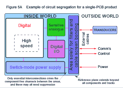 Figure 5A shows good segregation practices applied to a single-pcb product, whether it has an overall enclosure shield or not. This example shows that the segregated area where the outside world interface suppression components are fitted, is along one edge of the PCB, as if it were a wall between outside and inside-worlds (which it is, in a way).
This area would only contain opto-isolators, isolating transformers, baluns, filters, transient absorbers, similar interfacing components but no ICs. It would also contain bonding points for the screens of any screened cables, and/or for any enclosure shielding. If this example PCB was part of a larger assembly, the segregation techniques employed for best EMC would be just the same.
The inside/outside-world interface components are restricted to one dedicated edge of the PCB to encourage all unwanted external currents (e.g. caused by voltage differences in protective earths) to restrict themselves to that area of the PCB, and discourage them from flowing through circuit areas.
Where an effective enclosure shield exists, the inside/outside-world boundary becomes the shielded wall of the enclosure. All of the associated filtering and suppression components, and cable screen bonding, must then use a connector panel set in the wall of the enclosure as their reference (as described in Part 4). A single area for all interconnections is still best. A wider range of PCB-mounted screened and/or filtered connectors that can also bond to a metal panel is now available. These parts would be soldered to the PCB reference plane, then electrically bonded metal-to-metal to the wall of a screened enclosure during final assembly, and can be very cost-effective.
Narrow channels free from components should be left between each of the segregated circuit areas on the PCB. These should be wide enough for the fitting of a PCB-mounted "tuner-can" shield, and provision should be made (at least on prototype boards) for bonding such screening cans to the 0V plane at frequent intervals (say, every 15mm) along all edges.
5.1.4 Component placement and routing of tracks
The most noisy or susceptible components in each area should be positioned first, as close to the centre of their areas and as far away from cables or wires as possible. Such components include clock generators and distribution (extremely noisy); bussed digital ICs (very noisy); microcontrollers (noisy); switch-mode power transistors and rectifiers and their chokes, transformers, and heatsinks (all very noisy), analogue ICs (sensitive), and millivolt level amplifiers (very sensitive). Remember (from Part 1) that even low-frequency operational amplifiers can be extremely susceptible to interference, even beyond 1GHz.
After the extremely short connections from components to reference planes, digital clock distributions (very aggressive signals) must be the next "nets" to be routed, and must be run on a single PCB layer adjacent to a 0V plane. These tracks must be as short as possible, and even so may need to use transmission-line techniques (described later). It may be necessary to experiment with component placement to achieve minimum track lengths. Where clock tracks are made longer than necessary to minimise skew, a "serpentine" layout is best.
Digital busses and high-speed I/O should be routed next, in a similar manner to clock tracks, deferring only to clock tracks and plane bonds where there is a conflict. Very susceptible tracks, such as those carrying millivolt transducer signals, should also be routed as if they were clock or data buss tracks, although they will always be in a different segregated area of the PCB. The later section on transmission lines describes what to do where critical tracks have to change layers.
All other types of analogue, digital, and power signals should also be routed according to how aggressive or sensitive they are. Where these characteristics are not obvious from a circuit analysis, probing a prototype with a wide-band oscilloscope (and/or spectrum analyser) with voltage or current probes will reveal which are the most aggressive, and injecting voltages or currents from a wideband sweep generator will reveal which are most sensitive. A loop probe can be most useful here, being able to inject signals into tracks without requiring connection of external equipment to potentially sensitive area of the circuit concerned.
All components and their tracks must be contained within their designated PCB areas. The only tracks to exit or enter an area are those that have to connect to other areas. If it has not proved possible to eliminate all the wires and cables inside a product, make sure that their routes are fixed so they can't stray into the wrong PCB areas.
It is best to check that segregation instructions have been followed on draft PCB layouts, well before PCB manufacture. An easy check is to count the tracks and other conductors which cross the dotted lines showing the segregated areas on the circuit diagram - there should be exactly the same number crossing the channels between areas on the draft PCB layout. Where PCBs have been autorouted it is usual to find additional tracks crossing area boundaries - these are often the source of much design heartache, so eliminate them right away by applying more skill to the track layout. Autorouting does not generally provide good layouts for EMC purposes.
5.2 Interface Suppression
EM disturbances can be radiated and/or conducted across interfaces between segregated areas, and shielding, filtering, or isolation techniques (such as opto-coupling) are used to reduce this to acceptable levels. To decide on the most cost-effective methods for each interface, they should be assessed for all the EM phenomena possible, given the operational EM environment and the emissions/immunity characteristics of the circuits concerned.
Don't ignore internal power supplies and other common connections such as 0Vs or grounds when considering interfaces between areas. Circuit designers abbreviate such connections on their circuit diagrams, often to invisibility, even though they provide the return current paths that are as important as the send path.
5.2.1 Suppressing outside/inside-world interfaces
Conductors passing from outside to inside-worlds may need the full range of suppression techniques - shielding, filters, isolating transformers, opto-isolators, surge protection devices, etc. As described above, best practice is to use a single PCB area or panel in the enclosure shield for all outside/inside-world interconnections and their suppression.
Visual displays (such as LCDs, LEDs, VDUs, moving-coil meters, etc.) and controls (such as pushbuttons, potentiometers, rotary knobs, etc.) are also interfaces between outside and inside-worlds, and are particularly exposed to personnel electro-static discharge (ESD), which will be covered by Part 6 of this series.
Shielding (See Part 4) may be applied to chips or areas of the PCB; the whole PCB; sub-assemblies of PCBs; entire assemblies of PCBs; or the entire product (listed in ascending order of cost and difficulty). The segregation methods described above help make low-cost shielding possible.
5.2.2 Interfaces between dirty/high speed/noisy and clean/sensitive/quiet areas
Determining the types/amounts of suppression to be applied to tracks and other conductors interconnecting different PCB areas needs an assessment of both the desired signals and the unwanted noise they may carry, plus the sensitivity of the circuits they connect to.
Digital clocks and data busses are aggressively noisy and should not be allowed in clean/sensitive/quiet PCB areas. Data intended for a sensitive area should be latched from its bus no closer than the boundary of that area, and the data busses themselves restricted to a noisier area.
Power distribution networks are often overlooked routes for conducted noise from one segregated area to another, as are "static" data lines, and other low-frequency signals. Digital control lines which remaining at logic 1 or 0 for long periods are often thought to be quiet, but they usually carry tens or even hundreds of millivolts of high-frequency noise generated by the electrical activity of their source ICs (e.g. by "ground bounce" and its corresponding "power bounce"). Many an analogue circuit has suffered from noise on its power supply rails from switch-mode power supplies or DC/DC converters, or from digital processing sharing the same rails or from noise injected into analogue switches and opamps from "static" logic control signals. It is often necessary to fit small filters to such inter-area connections, but sometimes more drastic measures are required, such as opto-isolation.
Components that interface between segregated areas, such as analogue-to-digital convertors, transformers, data bus latches, filters, isolators, and the like, should be positioned at an edge common to the areas they interconnect. They should usually remain wholly within one area or the other (so as to keep a component-free channel) and their tracks must route directly to their respective areas and not mingle with tracks associated with the "other side" of these components or other areas.
Radiated interference between segregated areas is possible. The stray capacitance between components may only be a fraction of a pF, but at high frequencies can inject significant displacement currents into components and tracks in neighbouring areas. Combining small-sized low-profile components with PCB reference planes, and placing the noisiest devices (e.g. clocks, processors, switch-mode power devices) and signals in the centres of their areas, can help avoid the need to shield PCB areas from each other.
5.2.3 Details of interface suppression techniques
Suppression techniques include:
- common-mode and/or differential mode filtering
- galvanic isolation using opto-isolators or transformers
- communications protocols (to improve bit error rate in the presence of interference)
- surge protection devices
- the use of balanced drive and receive signals (instead of "single ended")
- the use of fibre-optic, infra-red, wireless, laser, or microwave instead of copper cables
- shielding of areas, volumes, cables, and connectors
All of these are covered by other parts of this series. It is important to realise that on a PCB only a plane (described next) can provide a good enough reference at high frequencies to enable the full performance of filters, cable screens, and internal shields to be achieved on a PCB.
5.3 Reference planes
Due to their intrinsic reactance and resonances, tracks, wires, "star grounding", area fills, guard rings, etc., cannot provide an adequate reference for a PCB except at low frequencies (usually below 1MHz). For example, the rule-of-thumb for the inductance of PCB tracks on their own or single wires, is 1nH/mm. This means that just 10mm of PCB track has an impedance of 6.3 Ohms at 100MHz, and 63 Ohms at 1GHz. For this reason, only unbroken areas of metal conductor can provide an adequate reference up to 1GHz (and beyond), and these are called reference planes. In a PCB these are usually called power, ground, or 0V planes, but it is best to avoid the use of the words "ground" or "earth" in connection with EMC and circuits (reserving them for specific uses associated with safety bonding). As far as most EMC design techniques are concerned, a connection to the green/yellow protective earth conductor can often be more of a problem than a solution.
Reference plane techniques allow dramatic reductions in all unwanted EM coupling when used in conjunction with the other techniques described here. Reference planes are also essential for almost every other PCB EMC design technique to function properly.
5.3.1 Creating proper reference planes
A high-quality high-frequency reference must have a vanishingly small partial inductance, and can be created on a PCB by devoting one layer to an unbroken copper sheet, called a reference plane. A 0V reference plane would be used as the 0V (or "ground") connection for all its associated circuits, so that all 0V return currents flow in the plane and not in tracks. Power planes are created and used in a similar manner for power connections and their return currents.
0V reference planes must lie under all their components and all their associated tracks, and extend a significant distance way beyond them. The segregation and interface suppression techniques described above must still be followed even where a common 0V plane is used for a number of circuit areas.
Perforations such as leads, pins, and via holes increase the inductance of a plane, making it less effective at higher frequencies. "Buried via" techniques have been developed for cellphones, allowing interconnections between tracking layers without perforating the reference plane. For less demanding products a rule-of-thumb is that any gaps must have dimensions of 0.01 l or less at the maximum frequency concerned. For a good plane at 1GHz, (e.g. to help meet most of the present EU harmonised EMC standards cost-effectively) this rule implies that plane gaps should have dimensions </= 1.5mm (remembering that the velocity of propagation in FR4 is approx. half of what it is in air). "Sneaking" tracks into a plane layer is not allowed.
Unavoidable gaps in a plane must not merge to create larger ones. PCB design rules should size clearance holes so that for regular hole spacings such as DIL packages the plane "webs" between holes, as shown by Figure 5B.
 Tracks, area fills, guard rings, etc. forming part of the reference on signal layers can be used to good effect at high frequencies - but only when bonded to an underlying 0V plane with at least one via hole every 5 to 15mm (using a random allocation of spacings).
0V planes should extend well beyond all components, tracks and power planes. [1] recommends "the 20H rule": 0V planes should extend by at least 20 times their layer spacing. High-speed components (such as digital clocks, processors, and memory) and their signal tracks should always be placed near the centres of their segregated areas, well away from plane edges.
All 0V and power connections must bond immediately to their respective planes to minimise their connection inductance. Leaded components must have their through-plated holes directly connected to planes using thermal-break pads as shown by figure 5B (sometimes called wagon-wheels) to help with soldering. Surface mounted devices (SMDs) for reflow soldering have to compromise the prevention of dry joints or "tomb-stoning" with the need to minimise inductance of plane connections.
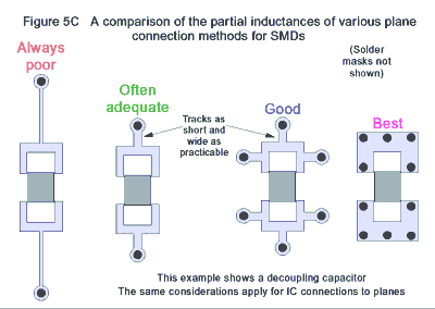 Figure 5C shows various methods for connecting reflow-soldered SMDs to planes. Best is to use over-sized pads, tenting the solder-resist over a number of plane vias. Plane connections that do not need to be soldered (typical of the vias for reflow-soldered SMD components) may not need to use thermal-break pads - and using solid plane connections instead will reduce inductance.
It is best to make reference planes rectangular (but not thin) to minimise their partial inductance, and also to make the fitting of PCB level shielding easier. Square planes, and planes with simple aspect ratios such as 1:2, should be avoided to help reduce possible problems with resonances. Where there are a number of different power supplies, there may need to be a number of different power planes. Segregation of circuit areas (see earlier) makes it easier to fit several broadly rectangular power planes on the same layer.
5.3.2 Connecting 0V planes to chassis
Components and tracks have weak capacitive coupling to everything else. Electrical activity causes displacement currents to flow in these "stray" capacitances, a cause of common-mode emissions. High-speed circuits usually need at least a nearby metal surface, and (increasingly) a fully shielded enclosure, to reduce the resulting emissions problems. The metal chassis or shields need to be connected to the reference plane of their PCB, preferably at a number of points spread over the PCB so that the high frequency displacement currents can be returned to their source within a fraction of their wavelength. PCB mechanical supports and fixings are often used for these chassis bonds, but should be very short (> 4mm). There should be at least one bond in the centre of each area of high-speed circuitry, especially clock generators and distribution. For high-speed digital boards, 0V plane to chassis bonds every 50 to 100mm all over the PCB may not be overkill, and provision (at least) should be made for these on prototype PCBs. Even if it is not intended to have a metal chassis or shielded enclosure, it is still a good idea to include a number of potential chassis bonding points, just in case. Sometimes a sheet of aluminised cardboard or PVC is sufficient to overcome unexpected problems, providing it can be bonded to the right place(s).
To add flexibility, especially for mixed analogue/digital PCBs, each plane-to-chassis bond can have tracks and pads that allow the bond to be left open, or else fitted with direct links or capacitors of various types and values. Fitting a direct link at one chassis bond and capacitors at the others allows low frequencies (for which the inductance is not important) to be controlled with a "star ground" system, whilst high frequencies are controlled by the low inductance of the widely distributed capacitive links. Care should be taken to minimise the inductances of all these tracks, pads, and linking components (SMD preferred). Where reference planes must be galvanically isolated only capacitor bonds may be used, but care should be taken with safety approvals and earth-leakage requirements (especially for patient-coupled medical apparatus).
5.3.3 Shielding effect of planes
Antennas placed close to metal planes are less effective at radiating and receiving. Many advantages of planes are due to the way they allow the return currents to take the path of least inductance, but their "antenna shielding" effect is also important. For any significant advantage to be achieved from this effect, the tops of all the PCB components must be no more than one-twentieth of a wavelength above a PCB plane, at the highest frequency of concern for emissions and immunity, e.g. 15mm to give a degree of shielding to analogue circuits exposed to 1GHz immunity testing.
Even lower profiles will give improved shielding, one reason why SMD components are much preferred for EMC, with very low profile ball-grid-array and flip-chip technologies being better still. The plane needs to extend by considerably more distance around the components than their height above it.
5.3.4 Interconnecting planes in multi-PCB assemblies
Card cage, backplane, and mother/daughterboard structures will experience considerable signal integrity and EMC advantages from linking their reference planes together with very low inductance. This may be achieved with frequent low-inductance links between their planes, more-or-less uniformly distributed along the full length of all their common boundaries. Shielded backplane connectors are happily becoming more commonly available. Where shielded connectors aren't used, using one 0V plane-linking pin alongside every signal or power pin in a connector may seem expensive, but sometimes it is the lowest-cost (or only practical) way to improve the EMC of a multiple-PCB product. Bonding planes via front panels and/or card guides is also very worthwhile.
5.3.5 To split or not to split?
Split reference planes may give better or worse EMC (and signal integrity) than unsplit planes, and this depends very much on the PCB layout and circuit design so it is often hard to decide which method to use. Note that where a 0V plane is to be split off from the main 0V plane, it may still need chassis bonds as described earlier. This is particularly true of "traditional" method of splitting off connector panel 0V plane areas (to try stop noise on the main board from exiting via the external connectors), when the connector area on the PCB must have its local 0V plane bonded to any enclosure shielding. Also note that the inevitable stray capacitance across a split progressively "shorts it out" above 500MHz anyway.
To get any benefits from split planes with modern electronic technologies requires significant attention to detail, which is one reason why an increasing number of designers are now using common, unsplit 0V planes as a matter of course.
Allow for both split and unsplit options, on prototype PCBs at least, by splitting all planes at the natural boundaries between the segregated circuit areas, but also providing the means to "stitch" them together manually later on. Stitching requires pairs of via holes on each side of the split every 10mm or so (random spacing of 5 to 15mm preferred). These via pairs may be left open, or bridged with short wires or capacitors, and it is important to pitch the via pairs close together so that small capacitors or "zero-ohm links" can be used (preferably SMD). Linking planes with a single copper link and multiple capacitors can control lower frequencies (where inductance is not significant) by "star grounding", whilst also controlling higher frequencies by creating the effect of a single low-inductance plane.
Because a split in a plane is a slot antenna, it is best if no tracks cross the split (or even go near to it). Where tracks have to cross - they must have carefully-defined return current paths, and for high frequency currents these paths must be physically adjacent to their send tracks. These tend to defeat the purpose of the split, so should be limited to the bandwidth of the wanted signal (which should already have been restricted to just what is needed, as described in the section on interface analysis and suppression above). High-speed signals can usually be returned through a suitable size and type of capacitor, although some data streams with highly-variable content may need a more wideband return path than a single capacitor can easily provide (may need a direct link).
Balanced signals would ideally need no local return path, but in practice their balance always degrades at some frequency so a nearby return path is needed for the resulting common-mode "leakage" (usually a small-value capacitor). DC power and low-frequency signals that have been filtered to remove all high-frequency noises can use the star point between the split 0Vs for their return, as long as the inductance of the resulting current loop is negligible. Beware of assuming that a conductor is only carrying low frequencies just because that is what its signal name implies. In modern mixed digital/analogue products all the tracks and other conductors in a product usually carry significant levels of high frequency noise. A local return path for a low-frequency signal could be a ferrite bead.
Common-mode (CM) chokes fitted to any types of signals and their associated returns (e.g. a 4-circuit CM choke for a set of three related signals and their return) will probably help get the best performance from split planes, but cost more.
When all the above has been designed into the split-plane PCB, it will need testing and optimisation. Direct or capacitive links to/from the "stitching vias" should be added/subtracted to achieve the best EMC performance. If it is discovered that the best EMC is achieved when all the stitching points are directly linked, the next iteration of the PCB could remove the splits and their stitching points completely, saving manufacturing costs.
5.3.6 Galvanically isolated planes
The split planes described above are all ultimately powered from the same power rails (0V, at least), so there is a clear need for return current paths to be catered for every conductor (signal or power) that crosses from one plane area to another. It is often assumed that galvanically isolated areas have no return current requirements, but this is not so at high frequencies.
Galvanic isolation devices (opto-isolators, transformers, etc.) suffer from stray internal capacitance. A typical opto has 0.8pF internal capacitance, which provides a shunting impedance of only 2k Ohms at 100MHz, or 200 Ohms at 1GHz, which will clearly prevent signal isolation from being maintained at high frequencies. Transformers (especially in DC/DC power converters) tend to have even larger stray internal capacitances. Common-mode chokes may be used to improve the isolation at high frequencies, but struggle to increase it by an order of magnitude at 1GHz. There are also many other stray capacitances around to compromise isolation. So there is a need, at high frequencies, to provide a local return path for the displacement currents that flow in these stray capacitances, to prevent them from causing common-mode conducted and radiated emissions and immunity problems.
Because we usually only need isolation for low frequencies (usually only 50Hz) we can connect galvanically isolated planes to the main reference plane with a number of low-value capacitors (spread around the gap perimeter), so as to achieve the effect of a single reference plane for high frequencies and provide low-inductance local return paths for stray displacement currents.
Of course, great care may need to be taken with component approvals and leakage currents where safety is concerned.
5.3.7 What if multilayer PCBs are thought too costly?
In volume, four-layer PCBs now only cost between 20% and 50% more than two-layer. The use of planes usually turns out, in retrospect, to have been the most cost-effective EMC technique possible, especially when the overall financial break-even time and profitability of a product is considered.
An appropriate technique for low-density double-sided PCBs is to put all the tracks on one side, and a solid 0V plane on the other. For digital products, the lack of a power plane might require a number of ferrite beads in the power rails (see later), so it might not prove to be most cost-effective.
Where tracks must use both sides of a two-layer PCB, some EMC improvements may be had by "gridding" 0V tracks. This can be done by using a "maximum copper" or "area fill" on the 0V tracks of both PCB layers, which must run perpendicular to each other, "stitching" the resulting horizontal and vertical 0V areas and lines together with via holes wherever they cross to create a grid over the whole PCB area. Smaller grid sections are needed around the more sensitive or aggressive components, often difficult to achieve for leaded microprocessors but easier for SMD types. Time should be allowed for moving components and tracks around to achieve the best grid structure, but any grid will always be much less effective than a proper solid plane.
Single-sided PCBs are extremely difficult to make EMC compliant without enclosure shielding and filtering, except for circuits which naturally have very low emissions (low dV/dt and dI/dt) and also have naturally very high susceptibility (e.g. high signal levels and low impedances).
5.4 Power decoupling
The aim of power decoupling is to maintain the power supply impedance to each IC at 1 Ohm or less across the entire frequency range of interest (at least 150kHz to 1GHz for EMC). Some devices may need 0.1 Ohm or less over some frequency ranges for correct operation. Wires and PCB tracks have too much inductance to provide these low impedances, which require local capacitance of suitable quality.
5.4.1 Power decoupling techniques
A large decoupling capacitor (e.g. 100µF) should be fitted where power supplies enter or leave a PCB, and some smaller ones (e.g. 10µF tantalum or solid aluminium) should be "sprinkled" around the PCB on a "µF per unit area" principle, as well as being positioned near to heavy power usage such as microprocessors, memory, and other powerful digital ICs. These capacitors provide low impedance up to, say, 10MHz. Next, the power supplies to every IC should be decoupled very nearby using appropriate capacitor sizes and types. Where an IC has a number of power pins, each pin should have an appropriate decoupling capacitor nearby, even if they are on the same supply (e.g. Vdd).
Achieving good decoupling above 10MHz gets more difficult as frequency increases, because the inductance of component leads, PCB tracks, via holes, and capacitor self-inductance, inevitably limit their performance. The achievement of good power supply decoupling at higher frequencies using capacitors mounted close to IC power pins is discussed next.
The total local decoupling capacitance required depends on the IC's transient power demands and the tolerances of its DC power rails. VLSI and RAM manufacturers should be able to specify the values (and maybe even the capacitor types and preferred layout patterns) for their products, but note that they will probably have assumed an accurate 5V power supply - usually not true of real life.
The formula C(DV) = I(Dt), using the units Farads, Volts, Amps, and seconds, covers what we want to know. DV is obtained by subtracting the IC's minimum operational voltage (from its data sheet) from the worst-case minimum power rail voltage (taking account of initial tolerances, regulation, temperature coefficients, ageing drift, and the voltage drops in the power conductors). DV often turns out to be a mere +100mV. I is the IC's transient current demand from its power rail, which lasts for Dt. I and Dt are almost never found in data sheets, and must be measured in some reasonably sensible way with an oscilloscope. An obvious component of I is the device's output (load) current, but this is often negligible in comparison with "shoot-through" currents, also known as "transient supply current". There is no point in measuring I or Dt with greater than ±20% accuracy.
Where DV is low it may be cost-effective to increase it by improving the regulation of the power supply, and/or reducing the resistance of the power rails, rather than fit larger capacitors with their lower performance at high frequencies. This is a common argument for local power regulation.
5.4.2 Self-resonance problems
Self-resonance in capacitors stops them providing low impedances at high frequencies, with higher values generally being worse. The first self-resonant frequency (SRF) of a capacitor is a series resonance, and a rule of thumb for this is:,

where L = ESL (internal to the capacitor)
+ the total inductance of any leads + the total inductance of any tracks and/or vias.
1nH/mm may be assumed for leads and/or tracks from a capacitor to the power pins of its IC. The inductance contributed by 0V and power planes may be neglected when the capacitor is near to its IC. Decoupling capacitors generally become ineffective at more than 3 times their SRF, as shown by Figure 5D.
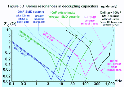
It is interesting to note that the favourite 100nF capacitor, even with no tracks at all, is effectively useless above 50MHz, yet it is still often seen in circuits with clocks of 50MHz or over, where it can do nothing to help control the fundamental clock frequency, never mind its harmonics.
Close proximity of adjacent 0V and power planes (with their low internal and connection inductances) can provide capacitance with no SRF below 1GHz. Two planes separated by 0.15mm in an FR4 PCB achieve approximately 23pF/sq.cm of high quality RF capacitor. Good decoupling from 10 to 1000MHz can be achieved by combining adjacent 0V and power planes with SMD ceramic capacitors (COG and NPO types are best). Sometimes two different values of capacitors (e.g. 100nF and 1nF) may be required. Low inductance bonds from IC power pins and decoupling capacitors to their planes is essential, and the capacitors must be positioned close to their IC. The common practice of tracking from IC power pin to decoupling capacitor, and only then connecting to the plane, does not make best use of plane capacitance.
Whenever two capacitors are connected in parallel, a high-Q (i.e. sharp) high impedance resonance is created which could compromise power impedance at that frequency. This is easily dealt with on PCBs which have a dozen or more decoupling capacitors, since for every sharp high-Z resonance there are a number of alternate current paths with low-Z, which will swamp it. It may be a good idea to fit decoupling capacitors of 10 to 100nF in large areas of planes which are devoid of ICs, to help this swamping process. Parallel resonances are very sharp and often don't correspond to any harmonics so have no effect, but unless it is known that this will also be the case for a new PCB (and that no-one will ever alter its clock frequencies) it is risky to ignore their potential for upset.
Parallel resonance problems are more likely to occur where only a few decoupling capacitors are used, for example where a small circuit area is powered from a dedicated power plane. It may be controlled by fitting a low-value resistor (say 1 Ohm) or small ferrite bead (preferably using SMD packages and short tracks) in series with one lead of the larger value capacitors. Alternatively, adding a number of additional capacitors with differing values should help.
The sudden change in characteristic impedance at the edges of parallel PCB planes creates resonances at integer multiples of half-wavelengths. For example, the first such resonance for a 150mm width or length would be around 500MHz for a bare PCB, moving down in frequency as the PCB was loaded with decoupling capacitors (which slows the velocity of propagation in the planes). This was the reason for recommending non-square rectangular plane shapes (and non-simple aspect ratios) in an earlier section. The resulting high impedances at various areas of the PCB can be controlled by fitting lots of decoupling capacitors, so it is only likely to be a problem for circuits operating at high frequencies with large planes and few decoupling capacitors. There is a suggestion that fitting 1 to 10nF decoupling capacitors around the edges of planes can reduce this effect.
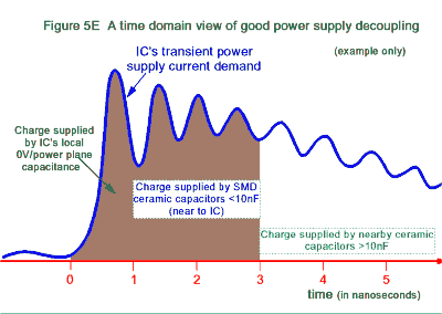
Figure 5E shows a time domain view of how good power supply decoupling functions in an example situation. The first nanosecond or so of transient current can only be provided by local 0V/power plane capacitance, with from 1 to 3ns being provided by SMD ceramic capacitors up to 10nF located nearby.
Larger (or further away) capacitors are only able to contribute to the current demand after at least 3ns. "Bulk" capacitors (e.g. tantalums) only provide significant current after 20ns or so, even if nearby (non-ceramic dielectrics and electrolytics are slow to respond to transient current demand due to dielectric absorption effects, also known as dielectric memory or dielectric relaxation).
A PCB process is available that uses a special dielectric between adjacent 0V and power planes to increase their capacitance and eliminate the need for most of the smaller values of decoupling capacitors. Three-terminal or "feedthrough" SMD decoupling capacitors have much higher SRFs than regular two-terminal capacitors, but are more expensive. There are also laminar capacitor components (such as the Micro/Q range) made to fit under leaded ICs, which are also expensive and perhaps best used in attempts to improve existing PCBs without relaying them.
5.4.3 Decoupling without power planes
One way to achieve possibly adequate decoupling without a power plane is to connect one end of an IC's decoupling capacitor to its power pin with very short fat track, then connect that end of the capacitor to the power distribution via a thin track (to create some inductance) or ferrite bead, rated for the IC's current. Three-terminal or high-specification capacitors may be used to advantage so that a high SRF is achieved with a single decoupler. This technique still requires a 0V plane. Where a large number of ferrite beads or expensive capacitors are required, multi-layer boards may prove to be more cost-effective and require less area.
5.5 Transmission Lines
Transmission lines maintain a chosen characteristic impedance, Z0, from a signal's source to its load, and (as discussed in Part 2) unlike all other interconnections do not resonate however long they are. Transmission lines can easily be made on PCBs by controlling materials and dimensions and providing accurate termination resistances at source and/or load. They may also be extended off the PCB (if necessary) with appropriate controlled-impedance cables and connectors.
A common rule of thumb is that transmission lines need to be used for signal integrity when the time that the leading edge of a signal takes to reach the furthest end of its track exceeds half of its rise or fall times. For example: Schottky TTL is specified as having 3ns risetimes, and in 3ns a signal in an FR4 PCB would travel about 450mm, so these signals should use transmission lines for tracks of 225mm or longer. Unfortunately, this rule is crude and can lead to problems if its shortcomings are not understood.
Databook specifications for output rise/fall times are maximum values, and most devices switch a lot faster. It is best to measure a number of samples from different batches, and obtain an agreement from the device manufacturer that he will warn in advance of mask-shrinks. Also, the inevitable capacitive loading from connected devices reduces the propagation velocity from what would be achieved on the bare board. So transmission lines should be used for much shorter lengths of track than suggested by the above rule, merely to achieve adequate digital signal integrity.
To improve EMC, and/or achieve a flat analogue frequency response, transmission line techniques may need to be used when tracks are one-half or less of the length actually required just for signal integrity. Taking all these caveats into account, we may find that specified 3ns rise/falltime signals should use transmission lines when they are any longer than 50mm (and possibly even less).
Transmission lines are often used for clock distribution and high-speed busses; for slower signals that have to travel further, such as SCSI and USB; and also for even slower communications such as 10base-T Ethernet and RS485, which have to travel very long distances.
IEC 1188-1-2 : 1998 [2], gives a wealth of details on constructing a wide variety of transmission lines with PCB tracks, plus how to specify their manufacture and check quality at goods-in. [1], [3], [4], and [5] are also very helpful with this large and detailed topic, so I will only briefly describe two of the most common types. It is possible to make transmission lines without planes, by using dedicated tracks for the return currents, but without very careful and expert EMC design the resulting track densities can be more a problem than using planes.
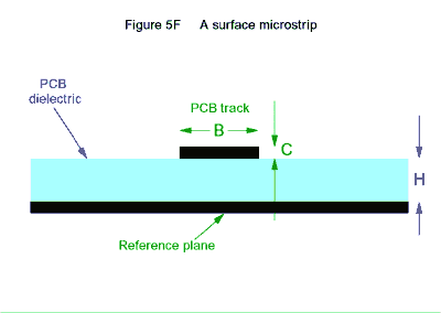
The first example is surface microstrip (see figure 5F), and its
Z0 is given in ohms by: 
where er is the relative permeability of the substrate (typically 4.4 for FR4 at 100MHz), B is the track width, C is the thickness of the copper material used, and H is the substrate thickness.
Its propagation velocity in ns/metre is: 
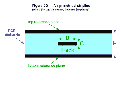
The second example is the symmetrical stripline (figure 5G), which uses two reference planes:  The propagation velocity for a symmetrical stripline in ns/metre is:
  Striplines are slightly slower than microstrip, but have zero forward crosstalk and much less off-board leakage, so are best for EMC.
[1] gives correction factors for the above formulae to compensate for capacitive loading (typically a few pF per gate):
 where Cd is the sum of all capacitive loads, Z0 is the original characteristic impedance (unloaded) of the line, and C0 is the characteristic capacitance of the (unloaded) line obtained from the basic formulae given in [2]. Velocity is slowed according to the formula:
 from [1], where V0 is the original
(unloaded) velocity. A constant "gates per unit length" is required, rather than bunching load ICs together (although the use of sophisticated CAD may allow the line-width to be adjusted to maintain the same Z0 along its length, even when ICs are bunched together).
from [1], where V0 is the original
(unloaded) velocity. A constant "gates per unit length" is required, rather than bunching load ICs together (although the use of sophisticated CAD may allow the line-width to be adjusted to maintain the same Z0 along its length, even when ICs are bunched together).
The highest-speed (or most critical) signals should run adjacent to a 0V plane, preferably one paired with a power plane for decoupling. Less critical signals may be able to be run against a power plane where the power plane has been adequately decoupled and is not too noisy (i.e. has been properly decoupled, see earlier). Any such power plane must be the one associated with the signal's ICs.
Transmission lines must not have any breaks, gaps, or splits in any of the planes they use, as these would cause sudden changes in Z0. They should also stay as far away as possible from any breaks, gaps, splits, or plane edges. Low crosstalk requires spacing adjacent transmission lines by at least three times their track width. A very critical or aggressive signal (e.g. a radio antenna connection) may benefit from using a symmetrical stripline with a row of close-spaced vias between its two 0V planes all along both its sides. This requires a different Z0 formula from those above.
High-speed or other critical transmission lines should not change layers. This means routing clock distribution first, moving components around to achieve the smallest area of highest-speed circuitry and tracks. High-speed busses, fast data communications, and the like are routed next, still sticking to one layer, and then everything else (less critical for signal integrity or EMC) is routed around them, changing layers as necessary. Where there is no reasonable alternative to changing the layers of a critical transmission line, a decoupling capacitor (with a suitable frequency response) should be fitted, with its vias linking all the relevant planes, near to the point where the signal changes layers.
5.5.1 Manufacturing issues with transmission lines
Normal FR4 PCB material has a nominal relative dielectric constant (er) of approximately 4.7 at 1MHz falling roughly in a linear fashion with increasing frequency to 4.2 at 1GHz. Actual values of er, can vary by ±25%. Controlled er grades of FR4 are available at little or no extra cost, but PCB manufacturers may not use these grades unless specifically requested. PCB manufacturers work with standard thickness laminations, and these should be discovered (along with their manufacturing tolerances) before design starts. The track widths can then be chosen to achieve the required Z0 for the available range of dielectric thicknesses. Track widths after PCB processing are usually about one thousandth of an inch less than those used on the photoplots. Ask what thickness to add to the drawn tracks to achieve the required finished track widths.
For signal frequencies greater than 1GHz it may be necessary to use other dielectric materials than FR4, such as those used for microwave applications.
5.5.2 Terminating transmission lines
"Classical" RF transmission lines are terminated both at signal source and load by impedances equal to their Z0 (allowing for the internal impedances of source and load devices). Although an ideal and sometimes necessary technique, it halves the received voltage - so most ordinary analogue and digital circuits use low-Z sources and high-Z loads with the line only terminated at one end, to preserve signal levels.
RF engineers often use reactive components or even lengths of track as line terminations, but the terminations for wideband analogue and conventional digital signals require individual resistors, preferably SMD types for their excellent high-frequency performance. To get the best from SMD resistors they must be connected to the reference planes using low inductance techniques as shown by figure 5C.
Figure 5H shows the common termination techniques. Classical RF termination is still used for fast backplane systems, and serial or parallel data cables such as SCSI and Ethernet.
Where signals are restricted to a single PCB, series (source) termination may be used at the driver end of a transmission line, with the resistor chosen so that in series with the impedance of the output driver it matches the line's Z0. This method has the advantage of consuming little power, and is most suitable for lines with a single load device at their far end. Where other loads exist along the length of the line they experience "reflected wave switching" and their response may need to be slowed to prevent false clocking.
Parallel (shunt, or load) termination at the very far end of a line is used where there are a number of devices spread along the length of the line and they need to respond most quickly, and achieves "incident wave switching". Figure 5H shows the termination resistor connected to the 0V plane, but some logic families use other reference voltages (e.g. the positive plane for ECL). Parallel termination dissipates a lot of power, and may also load some IC outputs too heavily.
Alternative types of parallel termination include "Thevenin" and RC. Thevenin uses resistor values designed so that their parallel resistance is Z0 and they would provide a DC voltage at their junction equal to the average line voltage, to minimise power dissipation. Thevenin termination needs a properly decoupled power plane at all frequencies of concern so needs decoupling capacitors nearby. RC termination uses capacitor values between 10 and 620pF (typically) and only terminates the line for high frequencies. Because of the problems of capacitors (discussed earlier) it may be more difficult for an RC termination to equal the highest frequency performance of a parallel resistor or Thevenin termination.
"Active termination" uses a voltage regulator to drive an additional power plane at the nominal average value of the digital signals. A parallel line termination connects to this plane, which must be properly decoupled for the frequencies of concern. Electrically equivalent to the Thevenin method, this can save power by running the voltage regulator (which needs to be able to source as well as sink current) in Class AB.
Where a line is driven bi-directionally the compromise position for terminating resistors (series or parallel) is in the centre of the line, so such lines should always be kept very short and may not be able to run as fast as the device speeds may suggest.
When "star" connecting a number of individual series-terminated transmission lines, either use one termination resistor chosen so that the total source resistance equals the parallel combination of all the starred lines, or else use one resistor to match each line. The latter technique should be better. The star configuration may also be used to drive multiple parallel-terminated lines. In either case, the signal source must be capable of driving the parallel combination of all the lines' Z0s.
Many ordinary CMOS or TTL ICs were never designed for driving transmission lines, and have neither the drive capability or an output impedance that is equal when sourcing and sinking. It may be best to choose higher values of Z0 to reduce signal currents. An increasing number of devices are now available to drive transmission lines. For example backplane buss driver ICs are available with 25 Ohm output impedances, suitable for "star" driving four individual 100 Ohm, or six 150 Ohm lines. Some devices now have on-chip DC/DC converters which cause their unloaded outputs to achieve double the correct logic levels, so that when operated into a classically terminated line the received logic levels are correct.
The usual technique of running digital busses in horizontal runs on one layer, "via-ing" through to another layer with "stub" tracks at 90° to connect to load devices will ruin a transmission line, unless the stub lengths are kept to less than one-twentieth of the total line length. These stub lengths can be too short to use sensibly, so "daisy chain" tracking from the source to each load in turn (ending up with the parallel termination, in an incident wave system) is often the best buss layout technique.
5.6 Layer "stack up"
The above section on decoupling shows it is good EMC practice to provide 0V and power planes on adjacent layers and to maximise their capacitance by using a thin dielectric (say 0.15mm) between them. The above section on transmission lines shows that proximity to a reference plane is important for high-speed tracks. We can put this all together to decide how to stack up our PCB layers.
Four-layer PCBs often have their layers stacked as follows:
- Microstrip transmission lines and other critical signals
- 0V plane
- +5V plane
- Non-critical signals
Where more signal layers are required, a 0V and power plane "core" should be retained. Additional layers of high-speed signals may need additional 0V planes to be added, but high-speed clocks and data busses and similarly aggressive or very critical tracks should not swap layers.
Here is one of a number of possible stack-ups for an 8-layer computer motherboard:
- 0Vplane
- Most critical "offset striplines" and other signals, routed at 90° to layer 3) to reduce crosstalk
- Most critical "offset striplines" and other signals, routed at 90° to layer 2) to reduce crosstalk
- 0V plane
- +5V plane
- Non-critical signals routed at right angles to layer 7) to reduce crosstalk
- Less critical "offset striplines" and other signals, routed at 90° to layer 6) to reduce crosstalk
- 0V plane
5.7 Useful references
- M. Montrose, EMC and the Printed Circuit Board, design, theory, and layout made simple, IEEE Press, 1999, ISBN 0-7803-4703-X
- IEC 61188-1-2 : 1998 Printed Boards and Printed Board Assemblies - Design and use. Part 1-2: Generic Requirements - Controlled Impedance.
- IPC-2141, Controlled Impedance Circuit Boards and High Speed Logic Design, Institute for Interconnecting and Packaging Electronics Circuits, April 1996.
- T Williams, EMC for Product Designers, Newnes, Oxford, 1992, ISBN 0-7506-1264-9.
- H W Johnson and M Graham, High Speed Digital Design, a Handbook of Black Magic, Prentice Hall, 1993, ISBN 0-13-39-5724-1.
The next issue will contain the final part of this series, and will cover a number of smaller topics: ESD protection techniques, electromechanical devices, and power factor correction.
Keith can be contacted on:
Phone: 01457 871 605, fax: 01457 820 145, or
e-mail: karmstrong@iee.org
Archive Index
EMC Journal Home

© Nutwood UK Ltd 2001
|
Eddystone Court - De Lank Lane
St Breward - BODMIN - PL30 4NQ
Tel: +44 (0)1208 851530 - Fax: +44 (0)1208 850871
nutwooduk@nutwood.eu.com
|
|