
Design Techniques for EMC Part 6: ESD, dips, flicker, dropouts, electromechanical switching, and power factor correctionBy Eur Ing Keith Armstrong C.Eng MIEE MIEEE |
This is the final part of a series of six articles on best-practice EMC techniques in electrical/electronic/mechanical hardware design. The series is intended for the designer of electronic products, from building block units such as power supplies, single-board computers, and "industrial components" such as motor drives, through to stand-alone or networked products such as computers, audio/video/TV, instruments, etc. The techniques to be covered in the six articles are:
Table of contents for this part
Machinery ESD occurs when isolated metal parts rub against insulating materials, or have a flow of insulating liquids or gases over them. The metal parts tribo-charge until they discharge with a spark into something nearby which was not previously charged, equalising their potentials. Sparks created in this way by machinery can be very intense, especially when the metal part being charged is large and so has a large capacitance, which can store a large amount of charge.
Furniture ESD occurs when metal furniture (or parts of furniture) such as chairs, tables, cabinets, etc., become tribo-charged by friction against insulating materials. This may happen when the furniture is moved across a carpet or plastic floor covering, or because materials are rubbed against it, for instance when a person gets up from a chair.
Personnel ESD is caused by people becoming tribo-charged, usually by walking around. Walking on plastic floor coverings, synthetic carpets, etc., is the usual cause of personnel ESD. Few people can even notice sparks from their fingers which are under 2.5kV.
Spacecraft ESD is not covered here, although many of the techniques described will be applicable.
All these three types of ESD are very important in the manufacture of semiconductors and the assembly of electronic products, and in these areas great lengths are taken to prevent the three types of ESD from reducing yields. Machine ESD can be a big problem for process control automation. But personnel ESD is the only type of ESD which we find in EMC standards harmonised under the EMC Directive. ESD causes EMC problems in three main ways:
Some older test standards use an older human body model which only has a 5ns risetime, so its spectrum begins to roll off at 60MHz and it is not as aggressive a test as EN 61000-4-2. As high-speed measurement techniques improve, it appears that real ESD events may have risetimes faster than 700ps.
Testing to EN61000-4-2 (personnel discharge) involves the following:
Bear in mind that in dry climates personnel ESD events can easily exceed 8kV. 15kV or even 20kV is not that unusual during freezing winter conditions when the air is very dry, especially in heated homes and buildings without humidity control. So, meeting an ESD test at ±8kV is not a guarantee of freedom from actual ESD problems in the field, and the environment and needs of the users should be taken into account when ESD testing to help produce reliable products.
6.1.3 Design techniques for personnel ESD
All the design techniques described in the previous parts of this series help a great deal in improving the immunity of circuits to electric and magnetic fields, and so help circuits cope with the brief but intense bursts of wideband disturbances from ESD events. However, they are not usually enough on their own. The two main techniques for preventing ESD sparks from upsetting products are:
Plastic enclosures, membrane keyboards, plastic knobs and control shafts, plastic switch caps, plastic lenses, etc., are all pressed into service to insulate the product (especially the operator-interface areas and controls). A 1mm thickness of common plastics such as PVC, polyester, polycarbonate, or ABS, is usually more than adequate to protect from 8kV of ESD (check the breakdown voltage rating of the material in kV/mm of thickness). But since no practical enclosure is without seams, joints, and ventilation, the achievement of adequate creepage and clearance distances becomes very important. Creepage is the shortest path that a current would have to take if it 'crept' along all available surfaces to reach the vulnerable part, while clearance is the shortest path to the vulnerable part through air (metal parts encountered along the way counting for zero distance regardless of their dimensions).
Clearance is the easiest to deal with, because the breakdown voltage of air is usually around 1kV/mm. So as long as the distance from the tip of the ESD gun to the vulnerable part is at least 8mm (preferably 10 or 12mm to give a design margin) an ESD spark can't occur.
Creepage is more difficult, because the surfaces of plastics are always contaminated with mould-release chemicals, fingerprints, dust, etc., which attract moisture from the air and form a variable conductivity surface. Sparks from the tips of ESD guns are often seen to follow a random path over the surfaces of plastic enclosures, displays, keyboards, etc., sometimes for as long as 50mm as they follow the path of least resistance through the dirt on the surface of the plastic, eventually ending on a metal part. (Painted metal surfaces often show similar long random spark tracking, usually leading to a pinhole defect in the paint that it takes a microscope to see.) So it is very difficult to specify an adequate creepage distance which will protect from an ESD test, although more than 50mm is probably adequate except for polluted or wet environments.
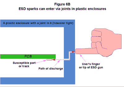
Figure 6B shows a combined creepage and clearance design issue. A joint in a plastic enclosure could allow an ESD spark to travel along the surfaces of the plastic, then through the air inside the enclosure to terminate on a vulnerable PCB track. Figure 6B shows that it is usually a good idea not to line up PCBs with seams or joints in their plastic enclosure.
LCD displays, membrane panels, and tactile rubber keypads can be very good at preventing ESD if a few basic precautions are taken. Although their surfaces are ESD-proof at least to 15kV, they can have problems at their edges. ESD sparks can track along the dirt on their insulating surfaces, and go around their edges to reach vulnerable internal tracks.
LCDs often dealt with this problem by using large bezels which prevented fingers from getting too close to their edges. Insulating sealant and similar materials are now more likely to be used these days. Another method is to surround the LCD panel with a metal bracket that 'catches' the spark before it gets to any sensitive parts, but then something has to be done to remove the charge from the metal surround without it discharging itself into some sensitive part. Membrane keypads and panels have internal conductive tracks, sandwiched between glued layers of plastic. If these tracks get too close to the edge of the panel, and if the glue has an airgap in it, sparks can track from the front surface (where the air discharge tip is applied), around the edge, through the void in the glue, and into the internal track, giving a false keypress if nothing worse. So whilst all attempts should be made to ensure there are no voids in the glue, it is still best to keep internal tracks at least 12mm from the edge of the panel (much more if possible).
Tactile rubber keypads also suffer from sparks that track through their surface dirt around the edges of their rubber mouldings and into the vulnerable keypad tracks behind. Unlike membrane panels, they usually don't have the benefit of glue to provide insulation, so it is important to extend the rubber edges of the tactile key moulding for far enough out, whilst keeping the tracks on the underlying PCB far enough in, so that any sparks have too far to go.
When a plastic enclosure has an internal shielding coating applied to meet RF emissions or immunity requirements, this can compromise dielectric isolation measures. For the conductive layers to make a connection across enclosure seams they must extend at least a little way into the seams, and may even be fitted with a conductive gasket. This can compromise the creepage and clearance distances that had existed on the unshielded version, and ESD tests on such enclosures often find that when the tip of the ESD gun gets anywhere near seams and joints in the enclosure, a spark flies from the tip and disappears into the seam or joint to meet the internal shielding layer. In this situation it is usually very hard to achieve dielectric isolation for the whole enclosure, and the shielding method described next may have to be employed instead. Where possible it is a good idea to plan ahead so that plastic cases are designed to allow internal shielding to be added later without compromising the dielectric isolation ESD protection. This can be difficult to achieve, especially on small products.
6.1.5 Shielding
Shielding attempts to divert the (very large) ESD currents away from internal circuitry. In general it is not as good as dielectric isolation because it exposes all the external conductive connections (and possibly internal circuits too) to indirect ESD injection via 'ground lift'.
When an ESD spark occurs to a metal enclosure, for the first few microseconds the enclosure will be at a much higher voltage than any protective earth it is connected to. This local 'ground lift' decays as the charge on the enclosure leaks away through the inductance of any protective earth connections (usually several tens of µH). Where an enclosure is not connected to protective earth the charge on the shielded enclosure leaks away slowly through ionisation currents in the air around it, conduction through humid fabrics, and similar mechanisms. During the beginning of a ground-lift event, internal circuits may still be at their previous voltages and sparking may occur between the enclosure and internal parts. This is known as 'secondary arcing' and it can be as bad for semiconductors and signals as the original ESD spark.
As long as the internal circuitry can cope with the sudden change in potential of its enclosure they don't care whether they are at protective earth potential, or 8kV relative to it. So it is quite practical to make battery powered or double-insulated products withstand ESD events (even though they are not connected to earth), although their isolation from earth may create greater problems for their external interconnections (discussed later).
So, on its own, having an external shield is not enough. One solution to secondary arcing is to bond the internal circuits to the enclosure shield, using connections that have a low enough inductance to maintain a low voltage between circuit and shield during an ESD event. These connections are often direct bonds from the 0V planes in the circuit boards to the enclosure, but they could be capacitive connections instead.
Where an enclosure contains a number of interconnected PCBs, it is important to ensure that during an ESD event they all charge up to the enclosure voltage at the same rate. If one circuit board has a low inductance connection to the enclosure, whilst another has a high inductance connection, then there can be a substantial transient voltage difference between them. This would inject a pulse of current into the boards' interconnections, causing cause signal corruption if not actual damage. So it is always a good idea to bond the 0V planes in different boards together using a number of conductors (one reference conductor for every one or two signal conductors may not be excessive) to help prevent large internal voltage differences.
Dielectric isolation of internal circuitry from the metal enclosure is another way to prevent internal secondary arcing, and allows the bonds between 0V planes and the enclosure to have high inductances, or not exist at all. This method has its drawbacks for sensitive circuits, especially those operating at high impedance. The inevitable stray capacitances between conductors and enclosure injects pulses of current into the conductors during a ground lift, and this may be enough to corrupt an analogue signal or alter a logic state in such a way as to cause a failure. Internal screening of sensitive circuits may be needed (bonded to their local reference plane).
Where galvanic isolation of circuits from enclosure is used to protect sensitive signals from differences in earth potentials, usually where long external cables are involved, the isolation is usually only needed at mains frequencies so it is often possible to capacitively bond across the galvanic barrier (with suitably rated capacitors). This equalises transient voltages during an ESD event without compromising functionality. Where this method is unsuitable, an internal shield over the isolated circuitry, bonded to its local isolated reference plane, may be required.
Even tiny gaps or joints in enclosure shields are weak spots, because they divert the very large fast currents from the ESD spark as they flow around the enclosure, causing locally intense pulses of electric and magnetic fields to be emitted through the shield and into the enclosure. Looked at from the frequency domain, we would say instead that the high frequency components of the ESD event find gaps and joints useful as slot antennae, radiating into the enclosure. So it is important to keep all gaps and joints in shields to a minimum size, as described in Part 4 of this series. Even if they are very small, sensitive circuitry should be kept well away from them.
6.1.6 Adding impedance to signal lines
Some interface devices (such as some RS232 ICs) are claimed to withstand EN61000-4-2 testing directly on their RX and TX connections. But for the vast majority of semiconductors it is by far the best to protect them from the direct effects of ESD by using the dielectric isolation (insulation) or shielding techniques, described above.
But if for some reason circuit conductors really must be exposed to ESD sparks: using a series resistor or choke (as shown in Figure 6C) may allow the ESD injection into the circuit to be handled by an IC's own internal protection devices. This is only likely to be possible for interface or 'glue logic' devices, and can't be generally recommended for VLSI devices such as microprocessors not intended to connect directly to external cables.
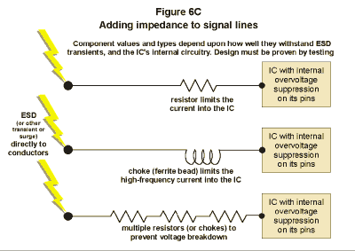
Most resistors or chokes aren't rated for ESD voltages, but may cope if they are physically large, have enough thermal inertia, and don't arc-over themselves. Since there is very little energy in a personnel ESD event, a large thermal inertia will prevent the resistor from suffering damage, although the same may not be able to be said of some machine ESD events involving large stored charge. It may be necessary to put a number of resistors or ferrites in series so that they share the ESD voltage and don't arc-over or break down (close to each other and arranged in a straight line, to get maximum advantage from this technique).
Since resistor and choke manufacturers don't specify their products' specifications on EN 61000-4-2 tests, it is best to check a few in a representative circuit and PCB layout. It may be found that different values may be needed for different ICs. The chokes used should be carefully chosen to provide a high impedance over the range of frequencies encompassed by the ESD event. Always perform a number of tests, to make sure that 'soft' failures aren't happening.
Mask shrinks by semiconductor manufacturers can make such a protective circuit design inadequate (just as it can invalidate all other EMC measures), so it is always best to have an arrangement with your semiconductor suppliers that they will warn you in plenty of time of any impending mask shrinks, so you can purchase some buffer stock to continue production whilst you evaluate all the EMC effects of the mask shrink, including any ESD protection.
The resistors or chokes may need to have such high values that they prevent the circuit from operating correctly. This is a particular problem for high-speed signals. One solution is to add discrete transient voltage suppressors, as described later. These will handle much larger voltage and current transients than most devices' internal protection measures, allowing series resistors or chokes to be reduced in impedance, or removed altogether.
However, a potentially serious problem for all methods that merely prevent fatal damage to semiconductors from direct ESD injection, is that they do not prevent momentary corruption of signals. Signal corruption can cause an ESD test to be failed, even though devices are undamaged. This is discussed later.
6.1.7 Transient Voltage Suppressors (TVSs)
As asserted above, it is always best not to allow sparks to get into circuit conductors. But if, for some reason, circuit conductors really must be exposed to ESD sparks: it may be possible to arrange for the associated ICs to survive by fitting series resistors or chokes as described above. An alternative technique that is widely advertised by TVS manufacturers is to fit suitably-rated discrete TVSs between the vulnerable conductors and the local 0V plane, a shown in Figure 6D. Being very much higher rated than an IC's internal protection devices, series resistance or chokes can have much lower impedance, and are often dispensed with altogether, which is sometimes much better for functionality.
Low inductance plane bonds are required for TVSs to protect ICs correctly, so the techniques described in Part 5 for connecting decoupling capacitors to 0V planes should be followed. Also, the PCB track to be protected must pass through the other terminal of the TVS. 'Spurring' a track from the signal path to a nearby TVS creates inductance which can prevent the TVS from protecting the IC. Since the TVS is required to bypass the powerful discharge current from the signal conductor into its local 0V plane, care must be taken that the ESD transient discharge current - now flowing in the 0V circuit and looking for a route back to the external earth - does not cause problems elsewhere in the product.
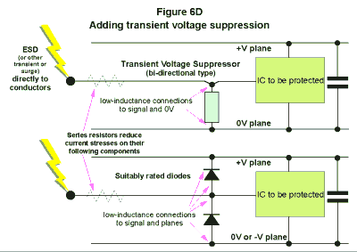
TVS components are now available in a wide range of voltage and power ratings, in leaded and SMD styles. They are also available as space-saving PCB-mounted arrays, and also fitted into connectors where they shunt the spark current into the metal body of the connector (which therefore needs to have a good high-frequency bond to the metal enclosure or the PCB's 0V plane). Some manufacturers make very thin flexible circuits which fit over the solder pins of common connector types, allowing an easy TVS retrofit to every pin of the connector. A big advantage of discrete TVSs over filtering is that they do not compromise high-speed signals as much. Most of them are based on zener technology so they do have some capacitance, and for very high speed signals the choice of an adequately low-capacitance TVS which still has the desired ratings can still be quite limited. Where extremely low capacitance ESD protection is needed, reverse-biased diodes between the signal conductor and the 0V and power planes, as shown in Figure 6D, can be effective. Reverse-biased diodes have a significantly lower capacitance than zener diodes. The diodes need to be able to handle the ESD currents when forward-biased, and the local power plane needs sufficient high-frequency decoupling capacitance so that its voltage does not rise too much when it absorbs the ESD charge. Where the leakage currents of TVSs or diodes are the problem, rather than capacitance, it is possible to use FETs instead to get nanoamp leakage.
Unfortunately, although TVSs are often advertised as a complete solution to problems of EN 61000-4-2 ESD sparks getting into exposed circuitry, this is not the case in practice. Their problem, which they share with the ICs internal protection devices and the reverse-biased diodes above, is that they cannot prevent the ESD transient from corrupting the signals on the conductors they are protecting.
Techniques additional to the use of TVSs are thus required to prevent signal corruption, and these are described in a later section.
6.1.8 Low-pass filtering the signal lines
Following a series resistor or choke with a capacitor to the local 0V plane (as shown by Figure 6E) can provide excellent protection from direct ESD injection to a conductor. As well as helping prevent actual damage, it can reduce transient voltages to such low levels that excessive signal corruption is prevented. Unfortunately, filtering has its limitations for high-speed signals.
A series 1k Ohm resistor followed by a 10nF capacitor to 0V would reduce a typical ESD pulse to very roughly 1/100th of its peak value (say 80V for an 8kV pulse) because the filter's 10 Ohms time-constant is very roughly 100 times longer than the ESD event. Peaks of 80V are probably within the capability of most ICs' internal protection devices, but signals would still be corrupted.
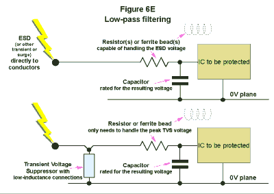
A 1ms time-constant (e.g. 10k Ohms in series then 100nF to 0V) would reduce an 8kV ESD event to very roughly 1/10,000th, say 0.8V peak, clearly well within any ICs ability to withstand, and usually low enough for a logic 0 not to be mistaken for a logic 1 (and vice-versa) in a standard 5V TTL system. A 1ms time constant is perfectly acceptable for keyboard interfaces, because it is almost impossible for an operator to press a key for less than 50ms in any case, but with a -3dB roll-off at around 150Hz it would be unacceptable for any audio applications.
Longer time constants can be used to achieve even less perturbation of analogue signals. 100k Ohms with 1µF would give a time-constant of 100ms, converting an 8kV ESD injection into a peak error of very roughly 8mV. Obviously, such high time constants can only be used on signals which are very slowly changing, but for many control lines and process-control parameters, a delay of 0.1s and a -3dB roll-off at 1.5Hz (or so) is unimportant.
Filtering after a TVS can be a good combination: the TVS reduces the ESD's 8kV (or whatever) to a few tens of volts, and the filter attenuates it to less than an important threshold whilst still allowing reasonably fast signals to pass. For example, a TVS that clamped ESD to 20V, followed by a 1k Ohm/10nF filter would reduce the transient voltage to (very roughly) 0.2V.
Where faster signals are required, filtering on individual lines can't be used, although common-mode filtering may well be possible (see later). Transient voltage suppressors may need to be used instead (see above), since they add only little capacitive loading, but it is still best not to let the spark get into the conductors in the first place.
6.1.9 Common-mode filtering at connectors
Because external signal and power cables are initially at their previous voltages, a 'ground lift' event due to a metal enclosure being struck by an ESD spark makes a transient high voltage appear across circuitry which interfaces with external cables. All things being relative, it is as if the enclosure was at earth potential and all its external cables had been suddenly raised to a high voltage. For example, if an enclosure was suddenly charged to +4kV by an ESD spark, it is as if the enclosure remained at earth potential but all the external cables had been suddenly charged to -4kV instead.
Although filters and/or TVSs may be used on each individual power or signal line, to help protect the electronics interfacing with the external cables (as described in the previous two sections), filters usually aren't compatible with high-speed signals, whereas TVSs can't prevent signal corruption (see later).
Because the transient voltage experienced by the interface circuitry is identical for all the conductors in a given cable it is a common-mode (CM) transient, and CM suppression techniques may be used to help suppress the transient voltage without compromising high-speed signals.

Figure 6F shows a common-mode choke used for this purpose. It needs as many windings as there are conductors in the cable. Surface-mounted and leaded common-mode chokes are available with up to eight windings. If the CM choke has a high enough value of common-mode impedance over the frequencies of concern it may be able to prevent an ESD transient from damaging the interface electronics. In situations where signal corruption is the problem, a CM choke can greatly reduce the signal perturbation.
When a CM choke is used with filter capacitors even greater suppression can be achieved, although this is not as suitable for high-speed signals unless quite small capacitor values are used (say between 10pF and 1nF, depending on the application). Where a large number of conductors must be accommodated specially-wound chokes may be required. A favourite technique is to pass the cable through a soft-ferrite cylinder or toroid. A single pass through a typical 32mm long ferrite cylinder creates a common-mode impedance of around 250 Ohms at 100MHz, not as much as some PCB-mounted components, but often enough to make a useful improvement to an EMC problem.
Where higher common-mode impedance is required, two or more turns of the cable could be made through the ferrite, each doubling of the number of turns increasing the impedance fourfold. Unfortunately, multiple turns also reduces the frequency at which the peak impedance is achieved, so beyond a certain number of turns no further benefit may be achieved from adding more turns. Multiple ferrites strung along a cable increase impedance proportionally to the number of ferrites, without reducing the frequency of the impedance peak, but can look a bit Heath-Robinson. Cables passed through ferrites should always finish on the other side of the ferrite from the side they entered, so that the ferrite is like a bead strung on a string, for best high-frequency performance.
6.1.10 Galvanic isolation techniques for ESD
Galvanically isolated external connections help a great deal with making products immune to ESD (and also to conducted transients and surges). PCB-mounted opto-isolators and transformers may be used, although many types will not have sufficient creepage and clearance and voltage withstand for ESD, and many types will have internal parasitic capacitances which may allow excessive transient currents to flow. Isolating mains transformers that meet their appropriate safety standards often seem quite adequate for protecting power supplies from personnel ESD, despite their shortcomings as ESD barriers.
The very best galvanic isolation for external signal communications is achieved with fibre-optic, wireless, or infra-red techniques, since these do not involve any conductors with dissimilar voltages being anywhere near the product concerned. Of course, the transmitting and receiving modules concerned can be very sensitive, and are often best fitted with their own local shielding, but even quite large PCB-mounted shields are now available taped and reeled for automatic placement and so can be much more cost-effective than when such items required manual assembly. Fibre optic cables sometimes use metal strengtheners, armour, or metal vapour barriers, and these can compromise the creepage and clearance distances required for ESD protection so should be stripped well back from any connections with products, where it is not possible to avoid the use of such cables entirely.
Five years ago I began expressing the opinion that by 2005 people who used copper cables to connect signals between items of equipment would be thought rather old-fashioned, and I still believe that this timescale is correct.
6.1.11 Dealing with signal corruption
When ESD testing to harmonised EMC standards using the EN 61000-4-2 test method, it is normal for the requirement to be that the operational state of the product being tested (and its displays and stored data) is exactly the same after the test as before. This is usually also the case for other transient tests such as Fast Transient Bursts (EN 61000-4-4), Surge (EN 61000-4-5), and the various automotive transients described by ISO 7637.
Using an IC's internal protection or a TVS to protect against ESD (or other types of conducted transient or surge) does nothing to prevent signal or data corruption, and can result in the product's operational state, displays, or memory being different after the test, leading to test failure. Additional techniques are often needed to prevent signal corruption.
For ordinary control lines such as keyboards, 'debouncing' techniques (whether hardware or software, such as are routinely used to debounce mechanical contacts) can work very well. Low-pass filtering (see above) is a good old-fashioned 'debouncing' technique often used after a TVS.
High-speed data can't use powerful debouncing techniques, and some type of error-protecting protocol is usually required, although of course this slows down the data rate too. Even without an error-correcting protocol it often makes a big improvement to the immunity of a data communication link if codes such as 10000000 or 01111111 are not used, since this is the sort of corrupted signal that appears when an ESD transient event affects a static data line (a brief single transient followed by no data). Merely avoiding such obviously error-prone codes is no help when the interference comes in bursts, as is usual for non-ESD transients, or when an ESD event causes secondary arcing.
Some very comprehensive error-correcting protocols are now commercially available, and it is usually much more cost-effective and time-saving to purchase the necessary chips or software licenses than it is to try to develop your own.
Momentary corruption of analogue signals is sometimes acceptable, when all that results is a brief click in a headphone or momentary flicker of a meter needle. But where decision thresholds may be crossed, or where the analogue signal is put through an averaging routine or stored in a memory after digitisation, even a brief error in an analogue signal may be unacceptable.
Since analogue signals can't easily use error-correcting protocols, debouncing techniques (such as a low-pass filter) are often used. Where the analogue signal must use high frequencies, it becomes very difficult to filter the transient event from the signal, the more so as the accuracy required (equivalent to number of bits of resolution) is increased, so dielectric isolation or shielding techniques are necessary after all, to prevent the ESD transient from getting into the signal conductor.
6.2 Dips, flicker, dropouts, interruptions, and brownouts
AC power supplies all suffer from momentary reductions in voltage: these are called dips. Dips are often due to a load being connected to the same supply (the finite impedance of the supply turns load current surges into voltage dips) or fault switching in the power network. When they occur frequently they are called flicker, because of the visual effect they have on electric lighting. When a dip is deep enough is called a dropout. When a dip lasts a long time it is called a brownout. and flicker, which are limited to a maximum amount.
6.2.1 Immunity to dips, flicker, etc.
All electronic equipment should be made resistant to such disturbances, even though they are not yet called up by harmonised EMC standards. Like surges (which this series of articles has not dealt with in much depth) these disturbances have been well known and documented since public electricity supplies first existed (around 100 years ago) and a manufacturer would have a difficult time trying to explain how he had met the Protection Requirements of the EMC Directive if he had not at least designed (and preferably tested) to meet these known EMC issues.
Immunity to dips, flicker, and dropouts is usually easiest to achieve by making sure that the unregulated DC rails of a product's power supply has a long enough 'hold-up time'. When dips or dropouts last so long that they become brownouts or interruptions, the best technique is to ensure that the product cleanly ceases operation, cleanly restoring operation when the event has passed.
The word 'cleanly' used above means that, for example, audio power amplifiers do not output speaker-wrecking or audibly unpleasant instability, pops, clicks, or thumps. For a motor drive the meaning of 'clean' depends upon the application - it could mean (for example) that the motor should stop instantly, or that it should coast to a stop, and after the event it should either ramp up slowly, or does not restart until manually commanded. Brownouts can damage motors, by allowing them to stall and overheat, damaging their insulation, so motors should be protected even where the electronics that control them is unaffected by the brownout. A digital circuit should shut down in a way that does not compromise stored data (although in non-critical applications it is often permissible to lose temporary data).
The desired behaviour of equipment during brownouts and interruptions depends on the application, and may be critical in safety-related applications. Since the EMC Directive does not cover safety, where errors and malfunctions in safety-related systems can be caused by the effects of electromagnetic disturbances on electronic circuits, these must be dealt with under safety directives such as the LVD or Machinery Directives.
A great number of semiconductor devices are now available for monitoring power supplies and effecting a controlled shut-down and reset when unregulated voltage rails drop too low. Almost no products nowadays should rely on a simple resistor-capacitor-gate power-on reset circuit, because they have always been inadequate for protecting circuits from the full range of perturbations of the AC supply.
Some power-monitoring devices 'look-ahead' to predict that the unregulated rail is about to become too, producing a signal which inhibits read/write operations to memories of various types. This can prevent memories from being overwritten with garbage during an undervoltage situation, and in the case of brief events which don't require a reset can even allow temporary data stored in RAM to be maintained, enabling operation to continue as if no hiccup in the supply had ever happened.
Uninterruptible power supplies (UPSs) are an increasingly common way of trying to deal with power supply quality problems, but they are not a universal panacea. Their ability to cope with all AC power EMC disturbances without passing them on to the 'protected' product should be investigated carefully, as should their reliability performance. It has been known for the reliability of electronics to be reduced because the UPSs they were run from had lower reliability then the equipment they were 'protecting'. Having said that, properly dimensioned and reliable UPSs which use full-time double-conversion can be a great help in preventing power supply problems from disturbing the operation of equipment.
6.2.2 Emissions of dips, flicker, etc.
Emissions of current surges to the network must also be considered (especially since EN 61000-3-3 is due to become mandatory under the EMC Directive for all apparatus up to 16A/ø supplied in the EU after 1/1/2001).
The easiest way to deal with the most common cause of transient surge current is to limit the switch-on surge into DC power supplies by fitting resistors in series with power supply inputs to limit their switch-on current surges. The resistors are shorted out by relay contacts after the first second or two.
An alternative is to use negative temperature coefficient (NTC) resistive devices instead of a series resistor. NTCs have an initially high resistance, reducing to a low value after they have been warmed up by the passage of current. Their thermal inertia and hot resistance needs to be taken into account with the current taken by the product and the permitted maximum input surges. Don't forget that NTC devices can get very hot, and must not be allowed to melt plastics, damage other components or cables, or burn operators or service technicians.
Motors and other inductive components also draw heavy surges of magnetising current when voltage is first applied to them. A useful technique for these is the soft-start (sometimes called a ramp start) where the voltage is applied with a slowly increasing amplitude. This also has the advantage of preventing sudden switch-on torques.
Large audio power amplifiers and similar high-power control products can cause flicker problems, especially with heavy bass notes and similar low-frequency load variations. The best, if expensive solution is to run such equipment from their own distribution transformer, motor-generator set, or double-conversion UPS.
Increasing the size of the storage capacitors on the unregulated power rails can help, but all this actually does is filter-out the higher frequencies in the flicker. To eliminate all the mains flicker can require extremely large capacitors since (broadly speaking) it is usually necessary to reduce the rate of 'flicker' to well under 1Hz. A better technique is to run the unregulated storage capacitors at a much higher voltage than is needed for circuit operation, allowing all the extra voltage for DC ripple caused by the heavy load current demands. When linear regulation is used this worsens efficiency, so the method is more suited to switch-mode regulators where efficiency will stay high (although higher voltage ratings may be required for the power devices). This is not a filtering technique, although time-constants will figure in the design, but is perhaps better described as a charge/time-management technique.
It is often possible to use a (so-called) power factor correction switch-mode boost converter technique (see below) to achieve a similar result. These circuits always limit the response time-constant of their input current demand to « second or more, so can easily be used to achieve the charge/time management required for low emissions of flicker to the supply network.
6.3 Electromechanical switching
Every conductor stores energy in its intrinsic inductance, and inductive devices such as motors also store energy in their magnetic fields. When the flow of current is suddenly interrupted by breaking an electro-mechanical contact, such as a switch, relay, commutator, or slip-ring, the 'flyback' of this stored energy causes a spark due, to breakdown of the air as the circuit-interrupting contact first opens (or when it bounces after closing).
Sparks emit electromagnetic disturbances quite literally from DC to daylight, and many microprocessor circuit designers have been surprised by the ease with which their higher-frequency components can couple into their digital circuits (e.g. via coil-to-contact capacitance, or proximity of cables or PCB tracks) and crash their microprocessors.
It is best to avoid the generation of arcs and sparks by avoiding electromechanical switching completely. The use of solid-state relays, brushless DC motors, AC motors, and the like all help eliminate sparking, although some of these will add new EMC problems of their own.
6.3.1 Suppressing arcs and sparks at switches, relays, and contactors
Where sparks cannot be avoided, emissions standards will be easier to meet by making sure there are no more than 5 sparks per minute in the product, with a spark duration of 10ms or less (less than half a mains cycle, typical of a microswitch or fast-acting relay). In heavy industrial applications it also helps meet emissions standards if the total rate of spark production is less than five per minute, but spark durations of up to a second or two may be acceptable. Beware - although these rates and durations of sparks may be allowed by an emissions standard, they can still upset sensitive circuits so may not be desirable for operational reasons, especially where critical functions are being controlled or monitored.
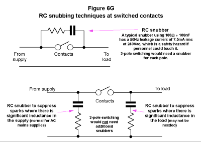
Emissions from arcs and sparks are usually reduced by 'snubbing'. Simple snubbing involves connecting a series combination of R and C (sometimes just C) near the switching element to slow the rate of rise of inductive flyback voltage and so limit the size of the resulting spark. Connecting a snubber across the contact gap has the disadvantage, in AC circuits, of allowing a leakage current to flow which might shock a person who worked on a circuit expected it to be safe because its relay contacts or switch were open.
Connecting snubbers in parallel with the load's send and return conductors, close to the switching element, sometimes gives better results than connection across the switched contacts, and does not allow leakage past the contacts. Sometimes two sets of snubbers may be required, one to deal with the flyback of the load's inductance, and one to deal with the flyback of the supply's inductance. Figure 6G shows the alternatives for snubbing switch and relay contacts.
Snubbers can also use non-linear devices such as diodes, rectifiers, zeners, and a variety of surge protection devices (see Part 3 of this series) to provide an alternative path for the flyback currents, either on their own or in conjunction with RC snubbers. The higher the turn-on voltage of the device, the faster the stored energy will collapse and the quicker can be the rate of cycling of the load. Unfortunately, the higher the turn-on voltage, the greater will be the spark at the contacts, so this can lead to a compromise between rate of operation and emissions. DC circuits can use unidirectional semiconductor snubbers, remembering that the flyback voltage has the opposite polarity to the applied voltage.
A side-benefit of all spark suppression techniques is that they generally increase contact life.
6.3.2 Suppressing arcs and sparks in DC motors
In general, DC motors are a very serious source of conducted and radiated emissions, and are very difficult to suppress. The filters and other suppression devices required for them to meet emissions standards can cost more than (and sometimes bulk as large as) the motor or bell itself.
Some 'pancake' DC motors don't spark because their brushes connect to a number of rotor windings at once, so there is always one of them in circuit to provide a path for the flyback currents in the windings.
Larger, more industrial DC motors with fully-enclosed metal bodies tend to emit less and be easier to suppress than lower-cost motors. Larger DC motors connected by many metres of cable to their controls or drives are able to reduce their emissions by using good quality screened cable, as long as its screen is 360o bonded at the motor's metal terminal box (and probably to the earthed cabinet enclosure at the controlling end).
Where this technique is not sufficient, or impossible to apply (as in many motorised toys or domestic equipment such as CD players), it is best to use a motor with transient suppression fitted to its rotor. The rotor is where the energy is stored in a brushed DC motor, and is best dealt with before it causes sparks in the commutator. A 'varistor disc' can easily be fitted to most low-voltage DC motors, essentially connecting a varistor (voltage-dependant resistor, described in Part 3 of this series) between each pair of contacts on the commutator. For a 24V motor the varistor disc may be designed to conduct at 30V or so, and only conducts current when flyback occurs. During flyback, it conducts the energy into the neighbouring winding and limits the resulting overvoltage at the commutator to under 45V or so. This still causes sparking, but only small ones with much lower emissions.
Where a varistor-disc motor cannot be obtained, it is usually necessary to shield the motor and filter after the commutator, not always very easy to do at low cost. Metal shielded motor bodies are preferred to (crudely) catch the radiated emissions from the sparks and return them back into the motor where they came from, via the filter. The filter is also needed to reduce the conducted emissions. Since DC motor emissions are still going strong at 1GHz (and also, in fact, at 10GHz), motor shielding needs to have very few very small gaps. Motors with metal end caps and metal bodies may appear well-shielded, but the bonds between the metal parts may be poor due to paint or anodising.
A filtering technique which works well is to bond one of the commutator terminals directly to the metal motor body (the shield). The other terminal is decoupled to the motor's metal body by a capacitor with very good high-frequency characteristics, such as an 820pF multilayer ceramic with a COG or NPO dielectric and very short leads. The capacitor must be rated to cope with the transient voltages caused by commutation. Where it is not possible to bond one of the brushes directly to the metalwork, it should be decoupled in the same way as the other brush. A low self-inductance is very important for these bonds and decoupling, and even 5mm of length or distance can be crucial. Feedthrough capacitors of around 1nF, screwed into the body of a fully metal enclosed motor and used as the brush terminals to the motor cable, often work very well indeed, although they are not inexpensive.
Correct application of shielding, bonding, and decoupling, may make the motor's emissions low enough. If not, the next step is to add chokes to the brush leads, as close as possible to the decoupling capacitors but immediately outside the motor body. Differential chokes and across-the-line capacitors may be needed to reduce low-frequency emissions, whereas common-mode chokes and line-to-chassis capacitors are usually best at suppressing high-frequency emissions. A multi-stage filter using both types of choke may be needed in difficult cases, and is often best implemented with a PCB mounted directly on the motor end-cap at the commutator end, to keep all lead lengths low and to permit low-inductance bonding of capacitors to the motor body.
A varistor-disc motor with only very tiny sparks on its commutator should last longer before it commutator wears out, whereas a shielded and filtered motor will not benefit in this way because its sparks have not been made any smaller.
6.3.3 Suppressing arcs and sparks in electric bells
Like commutator motors, electric bells create emissions from DC to daylight. The best technique is to remove their spark gap and use an oscillator (astable) circuit to pulse current through the hammer solenoid at the hammer's natural frequency. This is usually very much cheaper than any filtering methods. Such an electric bell could be much more reliable, and of course would require no adjustment to its spark-gap during manufacture. It may be that this is the first significant improvement in the design of electric bells since the 1880s.
6.4 Power factor correction
This is a topic that is exercising many power supply designers minds at the moment, since EN 61000-3-2 is due to come into force under the EMC Directive for all equipment under 16Amps/ø supplied in the EU from 1/1/2001. This emissions standard limits the harmonic (i.e. non-sine wave) currents drawn by products, and is particularly hard on linear and switch-mode DC power supplies used by almost all electronic products and equipment. It seems likely that single-phase linear power supplies above 100 or 200W will disappear entirely, except for "professional equipment over 1kW active power" for which a loophole will exist for a few more years.
The problem for typical rectifier-capacitor AC-DC power converter is that they only tops up their DC storage capacitors at the peaks of the AC supply waveform, so their supply currents are discontinuous, non-sine wave, rich in harmonics, with a poor power factor. This creates a number of problems for power generation and distribution, not least of which is overheating and fire, something that fire insurers are becoming increasingly aware of. There are a number of ways of dealing with this problem at the generation and distribution level, but only electronic design issues for equipment are covered here. Power converters with balanced loads running from three-phase supplies produce fewer triplen harmonics (3rd, 9th, 15th, etc.). Those running from six-phase supplies (two off three-phase supplies, one from a delta wound secondary and one from a star-wound secondary) have reduced levels of 5th and 7th harmonics too. There is a special problem for single-phase supplies, because they emit copious amounts of triplen harmonics, which are a particular nuisance since they add constructively, without cancellation, in neutral conductors and are a major cause of cable overheating. EN 61000-3-2 specifies very low emissions levels for the 3rd harmonic, which single-phase linear supplies will find increasingly hard to meet as their power increases above 50W.
Small linear power supplies have relatively high impedances in their mains transformers, which spreads their pulses of supply current in time and so reduces their harmonic content. As power transformers get bigger their impedance drops and the resulting current pulses into their bridge rectifiers are sharper and contain more troublesome harmonics. One solution is to add a series inductance, usually between the bridge rectifier and the storage capacitor. This helps widen the current pulses and so reduce their harmonic content. Lowest harmonics is realised when the choke has so much inductance that its DC current never drops to zero, but such a choke can be comparable in size with the isolation transformer. Also, calculations have shown that this technique alone can not theoretically achieve the 3rd harmonic emissions limits in EN 61000-3-2.
The remedial technique of choice for many designers is 'active power factor correction' - essentially a switch-mode boost converter between the bridge rectifier and the storage capacitor. This is sketched in outline in Figure 6H.
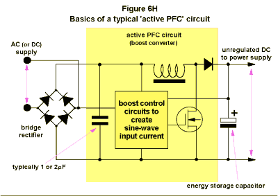
What circuits like that of Figure 6H do is to boost the full-wave rectified supply when it is lower than the voltage on the storage capacitor. The voltage is boosted so that the current into the storage capacitor approximates to a full-wave rectified sine wave. Thus the storage capacitor plus active PFC circuit looks like a resistive load to the bridge rectifier, and the whole lot appears to the AC supply like a resistor (although there are tiny discontinuities at the zero crossings due to the rectifiers). The boost circuit typically operates at a high frequency, even several MHz, so a filter capacitor (usually around 1µ F) is required to convert the fast-switching current pulses into a reasonably-looking rectified sine wave. When load currents vary suddenly, transient harmonic distortion of supply current occurs. To prevent this from causing a test failure, active PFC circuits have a time constant of around 0.5 seconds in their mains current input, and this needs to be taken into account when designing with fluctuating loads.
Of course, the boost circuit used generates high-frequency conducted and radiated emissions which need suppressing. Refer to Part 1 of this series for an introduction to EMC design techniques for switch-mode converters, and to Part 3 for an introduction to filtering. Usually these boost circuits are added to existing switch-mode power supplies, in which case some filtering and shielding may already in place, although they are likely to need modifying.
There is no reason why this type of active PFC circuit could not be fitted between the bridge rectifier and storage capacitor in the secondary side of a linear power supply. The voltages will generally be less, and the currents correspondingly higher. The term 'linear power supply' will then be better deserved, since traditional linear power supplies were always far from linear in their actual operation and the currents they consumed.
Disadvantages of active PFC techniques include their additional cost, weight, and volume, plus their additional emissions, but they have many advantages apart from helping to meet soon-to-be-mandatory harmonic emissions standards. These advantages include:
Theoretical background has been minimal, where it existed at all, despite the fact that an understanding of the theory behind emc helps designers deal with the unexpected (of which EMC often appears to have more than its fair share). The books recommended in Part 5 will be found useful in obtaining this knowledge. Many more EMC textbooks and guides exist for the interested reader.
Many of the techniques described in this series are also important for improving signal integrity. They are thus powerful competitive weapons in reducing the number of iterations during development, reducing manufacturing costs, improving reliability in the field and enjoying lower levels of product returns and warranty claims. They may also be helpful in reducing a company's risk under product liability legislation. Even if the EMC Directive did not exist in the EU, or the FCC in the USA, the techniques described in these six articles would still be worth using for the real engineering and financial benefits they bring.
Keith Armstrong can be contacted on:
Tel: 01457 871605
Fax: 01457 820145
eMail: karmstrong@iee.org
 © Nutwood UK Ltd 2001 |
Eddystone Court - De Lank Lane St Breward - BODMIN - PL30 4NQ Tel: +44 (0)1208 851530 - Fax: +44 (0)1208 850871 nutwooduk@nutwood.eu.com |
|
|
|